Touch Panel and Method for Manufacturing the Same

a technology of touch panel and manufacturing method, which is applied in the field of touch panel, can solve the problems of affecting the competitiveness of the market, the current level of input device technology exceeding the level of general functions, and the difficulty of efficiently operating products using the keyboard, etc., and achieves excellent adhesive properties and flexibility, and improves the flexibility of the transparent substra

Inactive Publication Date: 2012-12-20
SAMSUNG ELECTRO MECHANICS CO LTD
View PDF0 Cites 48 Cited by
  • Summary
  • Abstract
  • Description
  • Claims
  • Application Information

AI Technical Summary

Benefits of technology

[0011]The present invention has been made in an effort to provide a touch panel allowing the substitution of ITO by employing a metal mesh pattern as a sensing electrode and allowing the formation of the sensing electrode on a transparent substrate even without a separate adhesive layer by forming the transparent substrate of silicon having excellent adhesive property and flexibility, thereby improving flexibility of the transparent substrate, and a method for manufacturing the same.

Problems solved by technology

With the rapid advancement of an information-oriented society widening the use of computers more and more, the following problems come alight in that it being difficult to efficiently operate products using the keyboard and mouse as being currently responsible only for the input device function.
Furthermore, current techniques for input devices exceed the level of fulfilling general functions and thus are progressing towards techniques related to high reliability, durability, innovation, designing and manufacturing.
However, ITO has problems in that a raw material thereof, that is, indium is a rare earth metal and thus expensive, as a result price competitiveness is undermined, and besides, it is expected to run out in 10 years, and as a result, supply thereof will not go far enough.

Method used


Image

  • Touch Panel and Method for Manufacturing the Same
  • Touch Panel and Method for Manufacturing the Same
  • Touch Panel and Method for Manufacturing the Same

Examples


Embodiment Construction

[0030]Various objects, advantages and features of the invention will become apparent from the following description of embodiments with reference to the accompanying drawings.

[0031]The terms and words used in the present specification and claims should not be interpreted as being limited to typical meanings or dictionary definitions, but should be interpreted as having meanings and concepts relevant to the technical scope of the present invention based on the rule according to which an inventor can appropriately define the concept of the term to describe most appropriately the best method he or she knows for carrying out the invention.

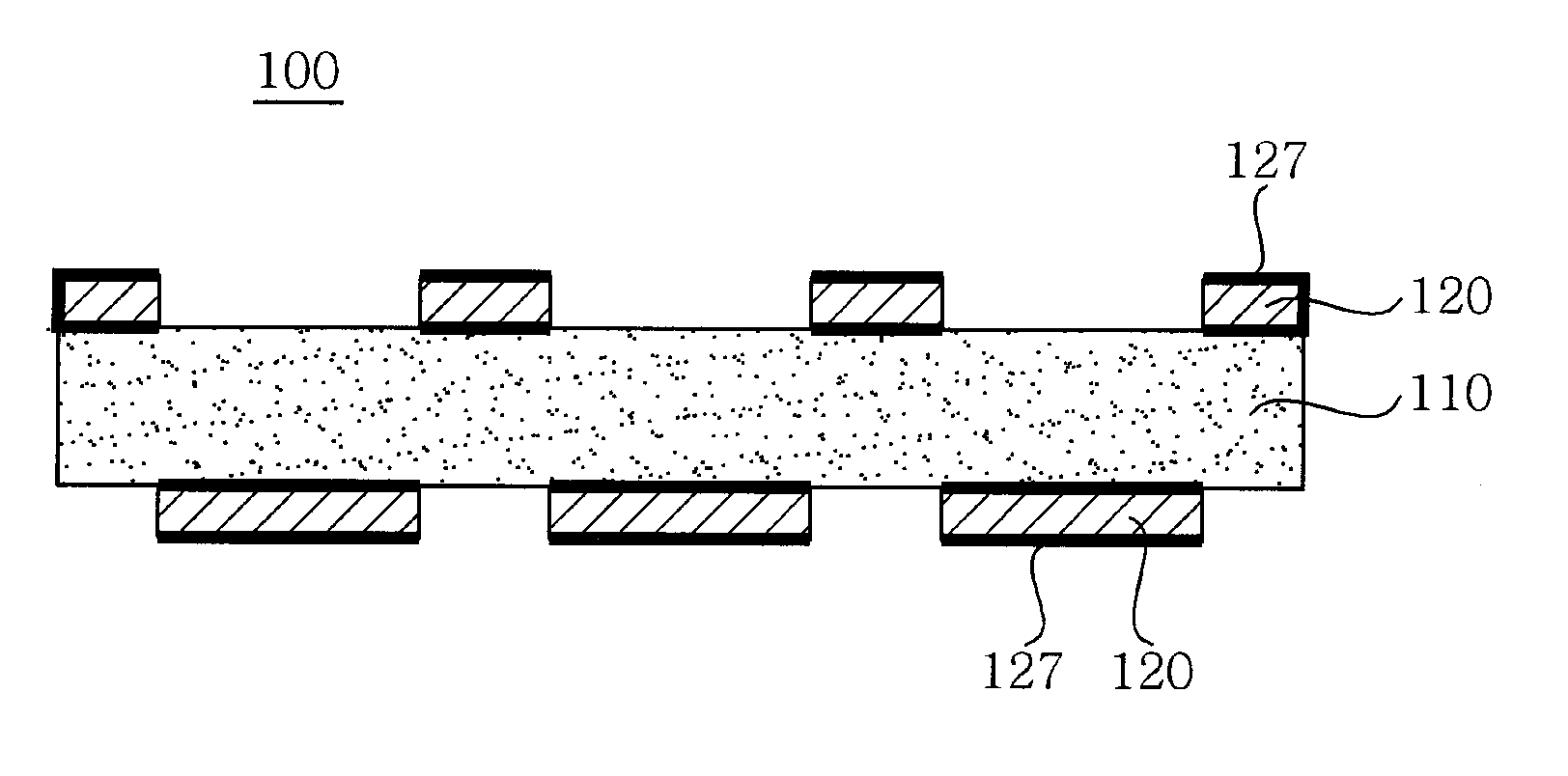
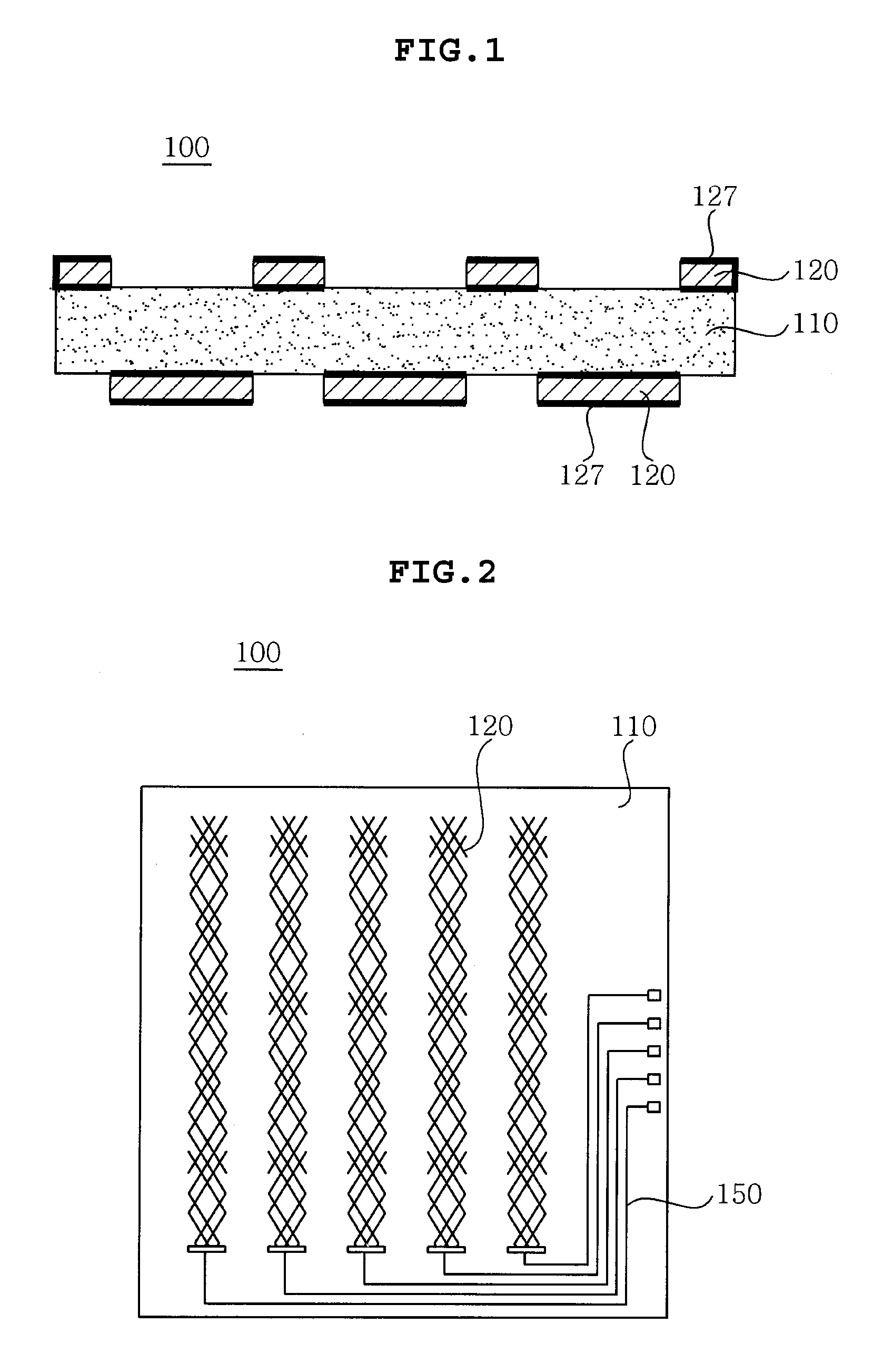
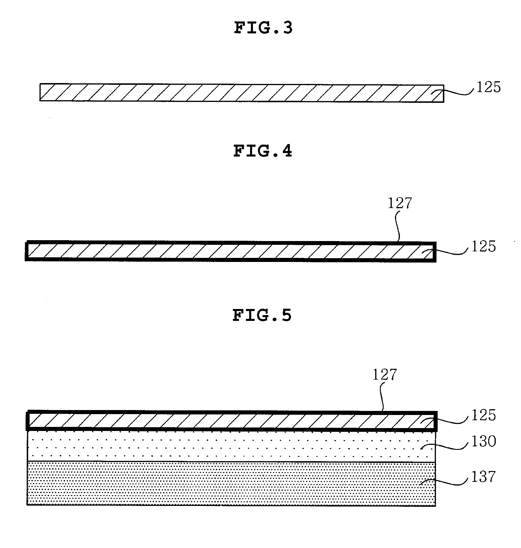
[0032]The above and other objects, features and advantages of the present invention will be more clearly understood from the following detailed description taken in conjunction with the accompanying drawings. In the specification, in adding reference numerals to components throughout the drawings, it is to be noted that like reference numerals designat...


PUM

PropertyMeasurementUnit
transparentaaaaaaaaaa
adhesive propertyaaaaaaaaaa
durabilityaaaaaaaaaa

Abstract

Disclosed herein are a touch panel and a method for manufacturing the same. The touch panel includes: a transparent substrate formed of silicon; and sensing electrodes each formed in a metal mesh pattern on one surface or both surfaces of the transparent substrate.Since the transparent substrate is formed of silicon having excellent adhesive property, the sensing electrode can be formed on a transparent substrate even without a separate adhesive material.

Description

CROSS REFERENCE TO RELATED APPLICATION[0001]This application claims the benefit of Korean Patent Application No. 10-2011-0057638, filed on Jun. 14, 2011, entitled “Touch Panel and Method for Manufacturing the Same”, which is hereby incorporated by reference in its entirety into this application.BACKGROUND OF THE INVENTION[0002]1. Technical Field[0003]The present invention relates to a touch panel and a method for manufacturing the same.[0004]2. Description of the Related Art[0005]As computers using digital techniques develop, computer assisted devices have also been developed together, and personal computers, portable transmission apparatus, other personal information processing apparatus, or the like perform text and graphic processes using various input devices, such as a keyboard or a mouse.[0006]With the rapid advancement of an information-oriented society widening the use of computers more and more, the following problems come alight in that it being difficult to efficiently op...

Claims


Application Information

Patent Timeline
Patent Type & Authority Applications(United States)
IPC IPC(8): G06F3/041H05K3/10
CPCH05K3/06H05K2201/0108H05K2201/09681Y10T29/49155G06F2203/04103G06F2203/04112H05K2203/0315G06F3/0412
Inventor KIM, JAE HUNKIM, SEUL GIHONG, SANG SUYANG, CHUNG MOLEE, IN HYUNGLEE, WOO JINLEE, YOUNG WOO
Owner SAMSUNG ELECTRO MECHANICS CO LTD
Why Eureka
Try Eureka