Method for manufacturing a semiconductor-on-insulator structure having low electrical losses, and corresponding structure
- Summary
- Abstract
- Description
- Claims
- Application Information
AI Technical Summary
Benefits of technology
Problems solved by technology
Method used
Image

Examples
Embodiment Construction
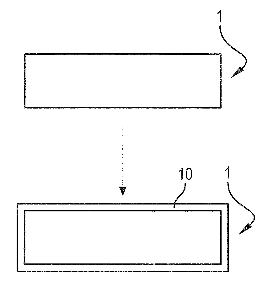
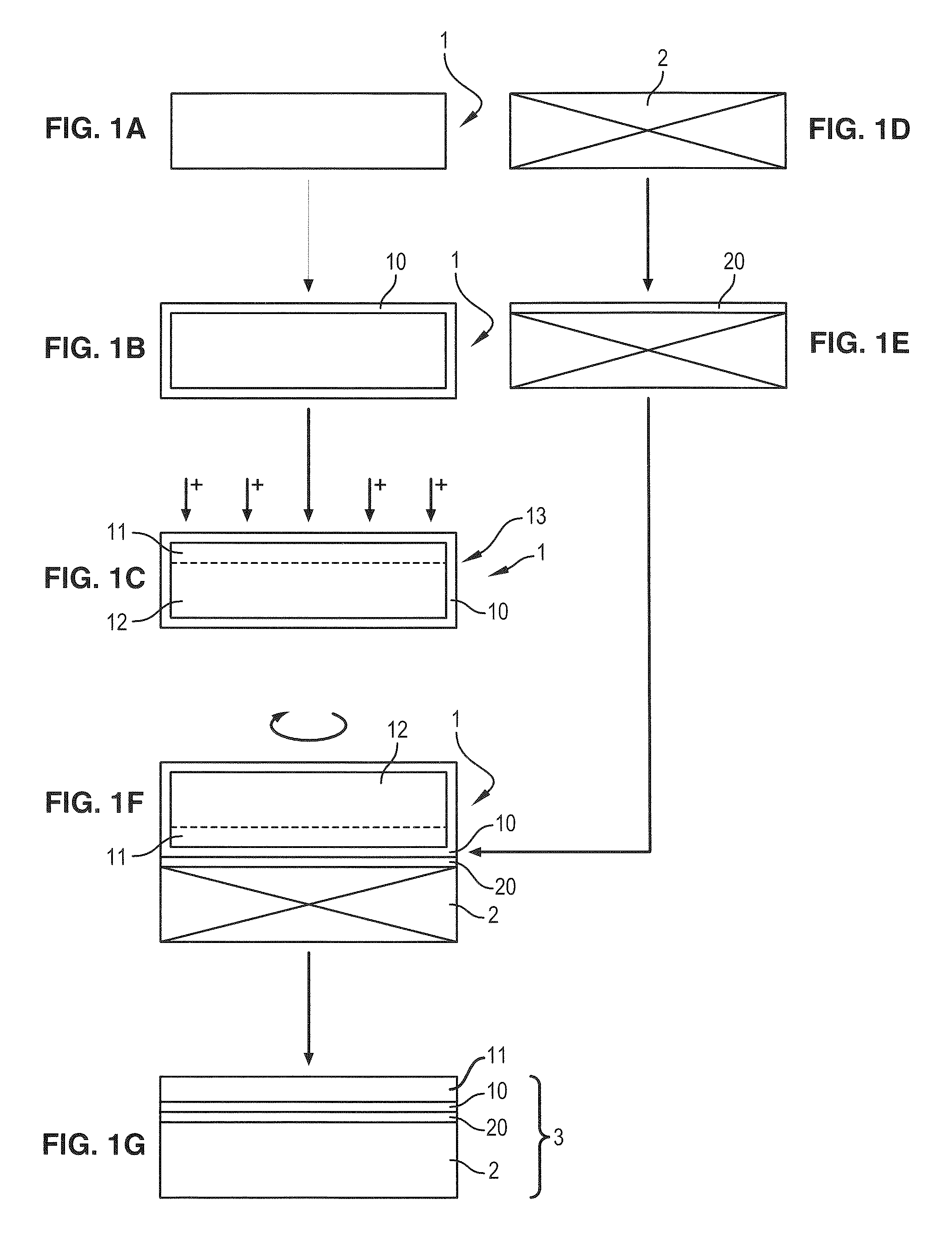
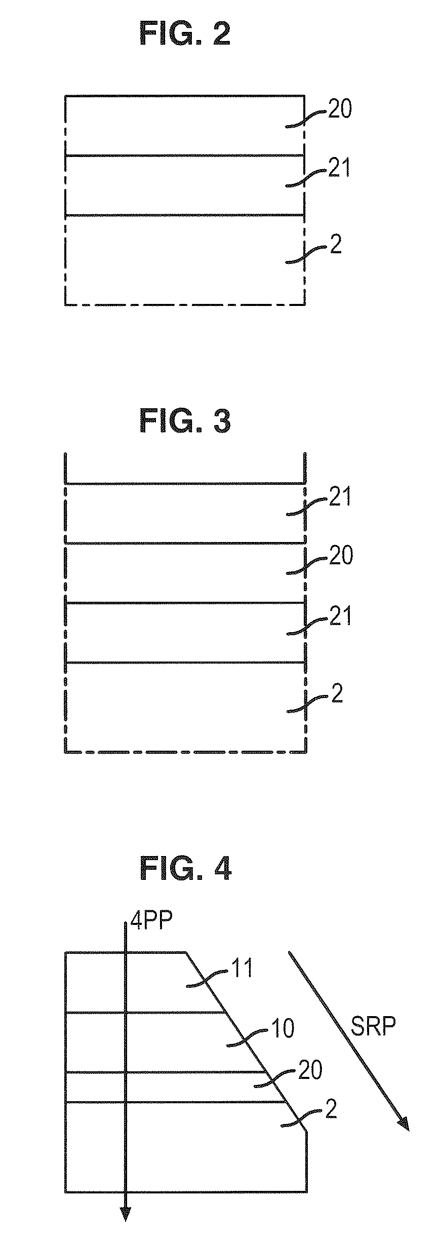
[0015]The present method is preferably applied to an SOI structure that successively comprises a support substrate made of silicon, a oxide layer and a thin layer of semiconductor material, a polycrystalline silicon layer being interleaved between the support substrate and the oxide layer. The process comprises the following steps:[0016]a) oxidation of a donor substrate made of semiconductor material to form an oxide layer at the surface;[0017]b) implantation of ions in the donor substrate to form an embrittlement zone therein;[0018]c) adhesion of the donor substrate to the support substrate, the oxide layer being located at the adhesion interface, the support substrate having undergone thermal treatment capable of giving it high resistivity, that is, a resistivity greater than 500 Ω·cm, its upper face which receives the donor substrate being coated by the polycrystalline silicon layer;[0019]d) fracture of the donor substrate according to the embrittlement zone to transfer to the su...
PUM
 Abstract
Description
Claims
Application Information
 - R&D Engineer
- R&D Manager
- IP Professional
- Industry Leading Data Capabilities
- Powerful AI technology
- Patent DNA Extraction
Browse by: Latest US Patents, China's latest patents, Technical Efficacy Thesaurus, Application Domain, Technology Topic.
© 2024 PatSnap. All rights reserved.Legal|Privacy policy|Modern Slavery Act Transparency Statement|Sitemap