Integrated circuit packaging system with underfill and method of manufacture thereof

a technology of integrated circuits and packaging systems, applied in the direction of electrical apparatus, semiconductor devices, semiconductor/solid-state device details, etc., can solve the problems of long time-consuming and laborious, difficult packaging-to-package stacking assembly process,

Active Publication Date: 2012-12-20
STATS CHIPPAC LTD
View PDF0 Cites 45 Cited by
  • Summary
  • Abstract
  • Description
  • Claims
  • Application Information

AI Technical Summary

Benefits of technology

[0007]The present invention provides a method of manufacture of an integrated circuit packaging system including: providing a substrate with a projection formed along a perimeter of a first surface of the substrate; mounting an integrated circuit over the first surface; forming a protruding interconnect over the first surface between the projection and the integrated circuit; and forming an underfill between the integrated circuit and the projection with a uniform height, the uniform height of the underfill less than a height of the projection.

Problems solved by technology

However, vertically stacked packages have their own problems, such as, local and global planarization inconsistencies, which makes the package-to-package stacking assembly process difficult due to the irregularities in the flatness or planarity of the packages.
Solutions to these problems have been long sought but prior developments have not taught or suggested any solutions and, thus, solutions to these problems have long eluded those skilled in the art.

Method used


Image

  • Integrated circuit packaging system with underfill and method of manufacture thereof
  • Integrated circuit packaging system with underfill and method of manufacture thereof
  • Integrated circuit packaging system with underfill and method of manufacture thereof

Examples


first embodiment

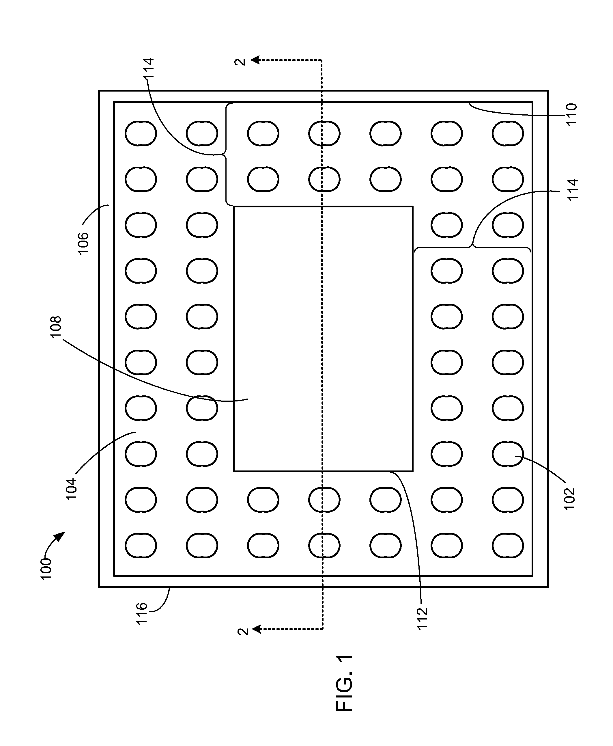
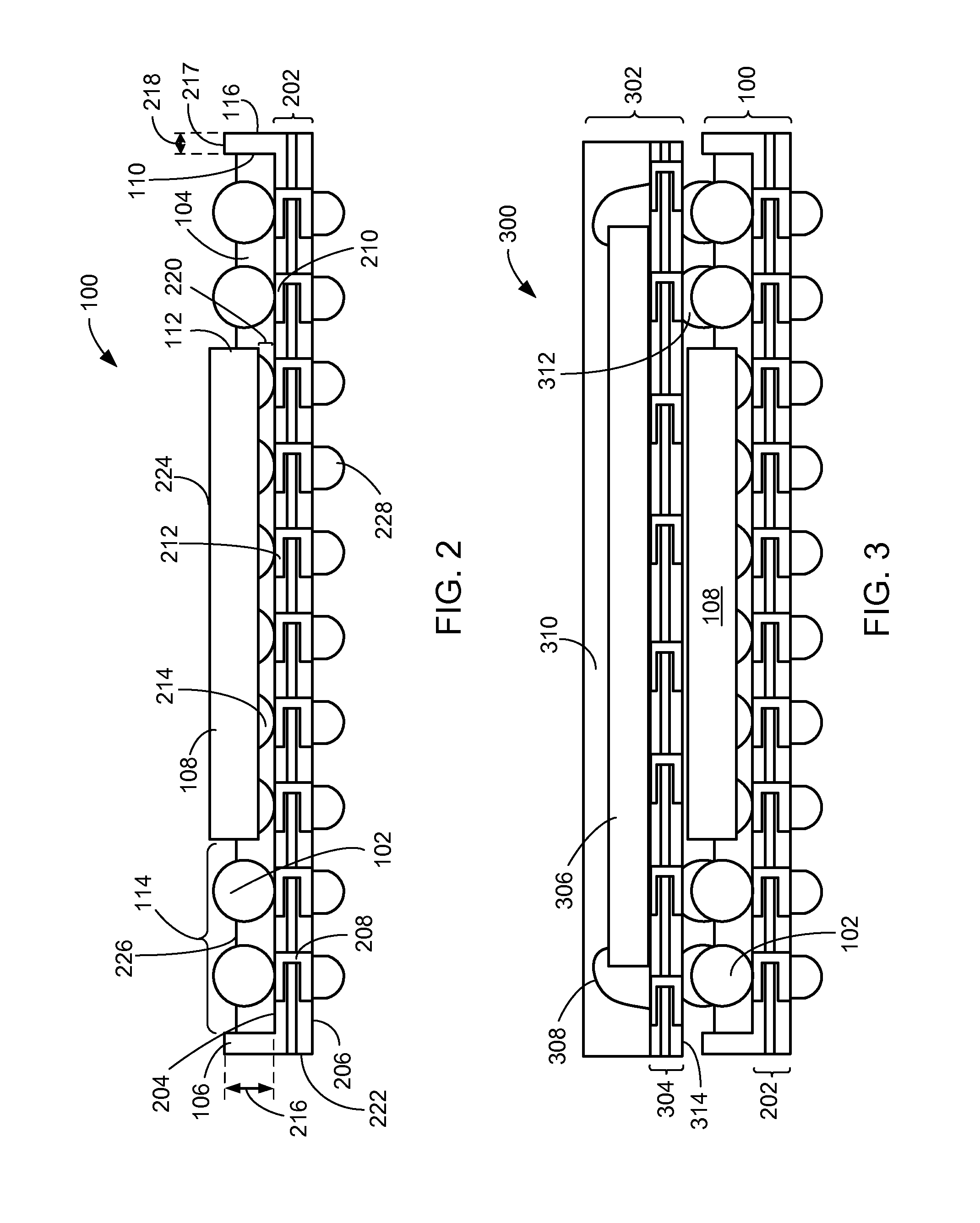
[0027]Referring now to FIG. 1, therein is shown a top view of an integrated circuit packaging system 100 in the present invention. In at least one embodiment, the integrated circuit packaging system 100 can include a bottom package, a base package, or a first package. In such cases, the integrated circuit packaging system 100 can be utilized within a package-on-package (PoP) configuration or packaged as a separate and discrete element. PoP refers to a 3D package in which fully tested packages are stacked on top of another single or stacked package during the board mount process. The integrated circuit packaging system 100 can provide electrical access to electrical circuits formed above and below the integrated circuit packaging system 100.

[0028]In at least one embodiment, the integrated circuit packaging system 100 is depicted as square in shape; however, it is not limited to such shape and can include any rectilinear or curvilinear shape.

[0029]The integrated circuit packaging syst...

second embodiment

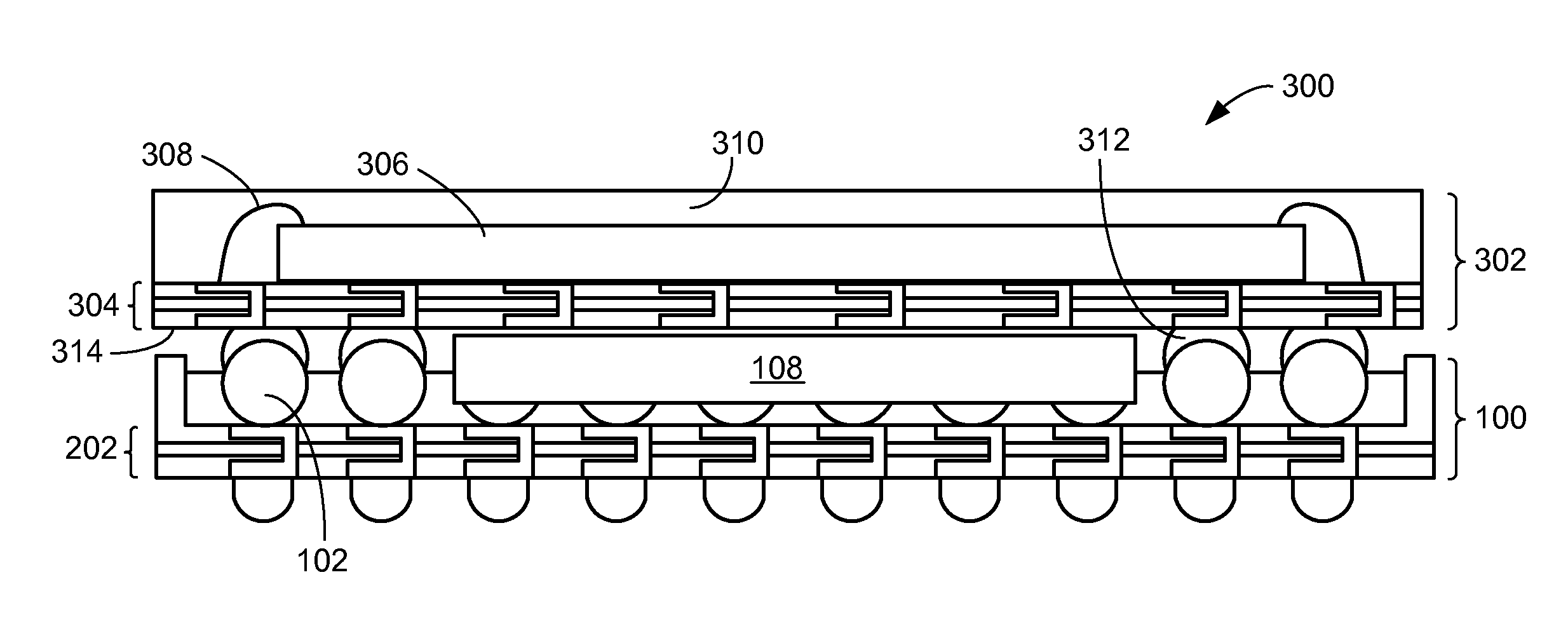
[0072]Referring now to FIG. 3, therein is shown a cross sectional view of an integrated circuit packaging system 300 in the present invention. In at least one embodiment, the integrated circuit packaging system 300 can include a package-on-package configuration. In such cases, the integrated circuit packaging system 100 can be referred to as a bottom package, a base package or a first package.

[0073]Formed over the integrated circuit packaging system 100 is a device 302, such as an integrated circuit, die, chip, integrated circuit package or other electronic circuit including both passive and active components. In at least one embodiment, the device 302 can be referred to as a top package; however, other electronic circuits or other packages can be formed over the device 302 as required by the design specifications of the integrated circuit packaging system 300.

[0074]Generally, the device 302 can include a substrate 304 similar to the substrate 202, of FIG. 2, and an integrated circu...


PUM


Abstract

A method of manufacture of an integrated circuit packaging system includes: providing a substrate with a projection formed along a perimeter of a first surface of the substrate; mounting an integrated circuit over the first surface; forming a protruding interconnect over the first surface between the projection and the integrated circuit; and forming an underfill between the integrated circuit and the projection with a uniform height, the uniform height of the underfill less than a height of the projection.

Description

TECHNICAL FIELD[0001]The present invention relates generally to an integrated circuit packaging system, and more particularly to a system for an underfill structure and application within an integrated circuit packaging system.BACKGROUND ART[0002]Integrated circuits and integrated circuit packaging systems can be found in a multitude of portable electronic devices, such as smart phones, pocket PCs, digital cameras, location based devices, and other wireless products. Today's customers and electronics systems are demanding the functional integration of memory and logic within the smallest footprint, lowest profile, and lowest cost package available. Consequently, manufacturer's are turning to three-dimensional packaging to achieve the required high level of functional integration necessary to support these mobile multimedia products.[0003]Integrated circuit packaging systems continue to advance toward miniaturization by vertically stacking packages in package-on-package configuration...

Claims


Application Information

Patent Timeline
Patent Type & Authority Applications(United States)
IPC IPC(8): H01L23/48H01L21/50
CPCH01L2224/73265H01L23/49816H01L23/13H01L21/563H01L2924/3511H01L2924/15331H01L2924/15311H01L2924/15153H01L2224/73204H01L2224/48227H01L2224/32225H01L2224/27013H01L2224/16225H01L2924/18161H01L2924/1515H01L2225/1058H01L2225/1023H01L25/105H01L2924/00012H01L2924/00H01L24/73
Inventor KIM, OH HANKANG, YONG HEECHOI, DAESIK
Owner STATS CHIPPAC LTD
Why Eureka
Try Eureka