Bump formation method and wire bonding method

a technology of wire bonding and bubbles, which is applied in the direction of soldering apparatus, manufacturing tools,auxillary welding devices, etc., can solve problems such as poor productivity, and achieve the effect of superior in terms of productivity and uniform height and shap

Inactive Publication Date: 2006-05-16
SHINKAWA CO LTD
View PDF7 Cites 21 Cited by
  • Summary
  • Abstract
  • Description
  • Claims
  • Application Information

AI Technical Summary

Benefits of technology

[0012]The object of the present invention is to provide a bump formation method and wire bonding method that allows the formation of bumps with a uniform height and shape and that is superior in terms of productivity.

Problems solved by technology

In other words, since a number of ball formation steps and wire cutting steps corresponding to the number of stages in the bump are required, this method has a problem of poor productivity.

Method used


Image

  • Bump formation method and wire bonding method
  • Bump formation method and wire bonding method
  • Bump formation method and wire bonding method

Examples


first embodiment

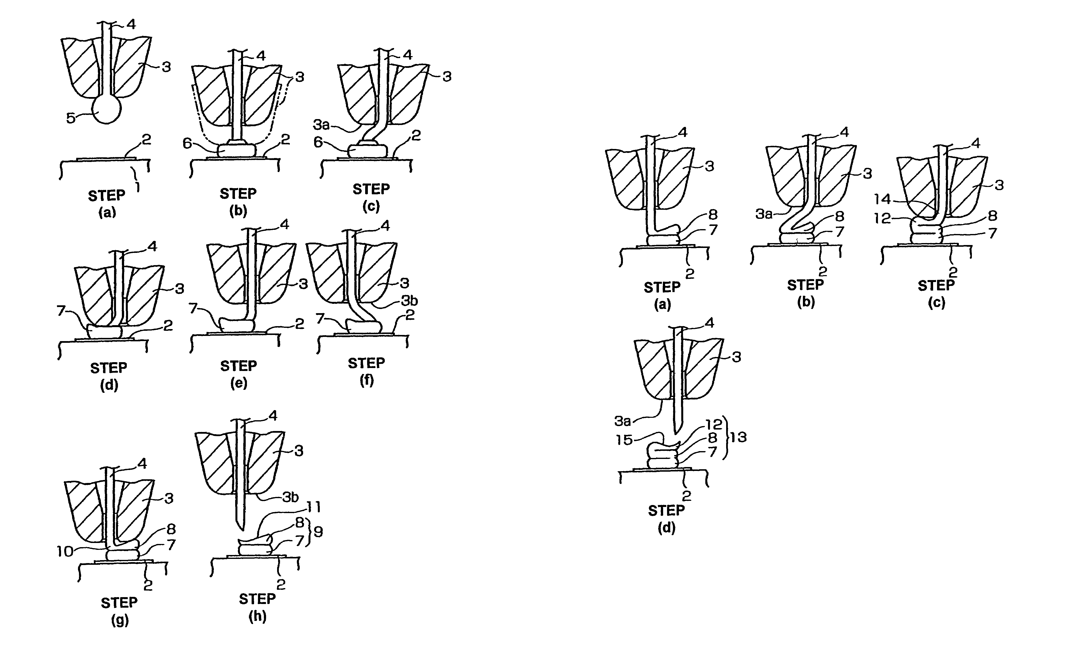
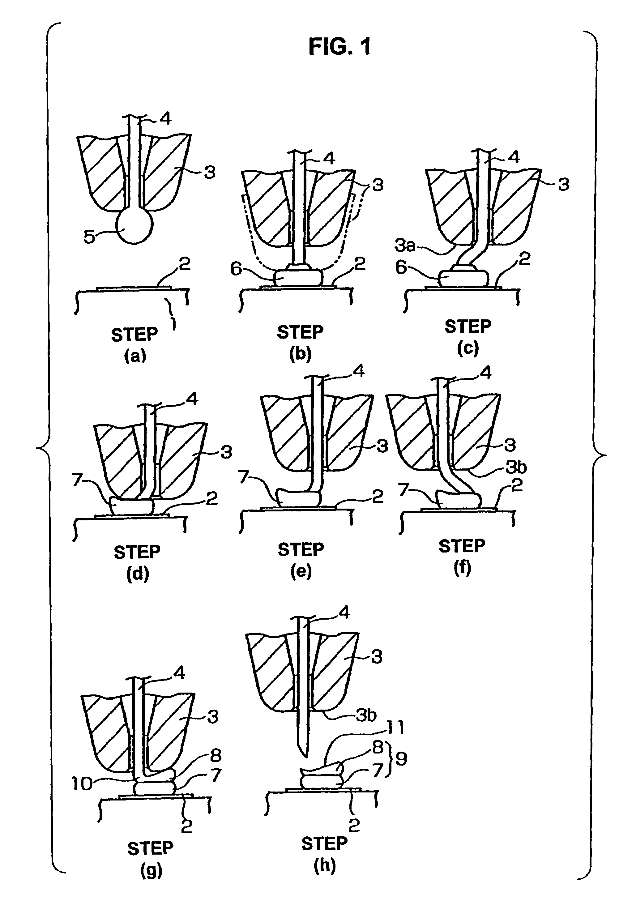
[0023]the present invention will be described with reference to FIG. 1.

[0024]In FIG. 1, the reference numeral 1 indicates a semiconductor element, and 2 indicates an electrode pad 2 which is formed on the surface of the semiconductor element 1.

[0025]As seen from step (a) in FIG. 1, a ball 5 is formed by a spark discharge, etc. on the tip end of a wire 4 that passes through a capillary 3, in a state in which a damper (not shown) is closed.

[0026]Next, in step (b), the damper (not shown) is opened, the capillary 3 is lowered as indicated by the two-dot chain line, and the ball 5 is joined to the surface of the electrode pad 2 by ultrasonic vibration, so that a press-bonded ball 6 is formed (or the ball 5 becomes the press-bonded ball 6).

[0027]Next, the capillary 3 is raised as indicated by the solid line in sep (b); and then in step (c), the capillary 3 is moved in the horizontal direction (to the right) so that a flat portion 3a on the lower end of the capillary 3 is positioned to fac...

second embodiment

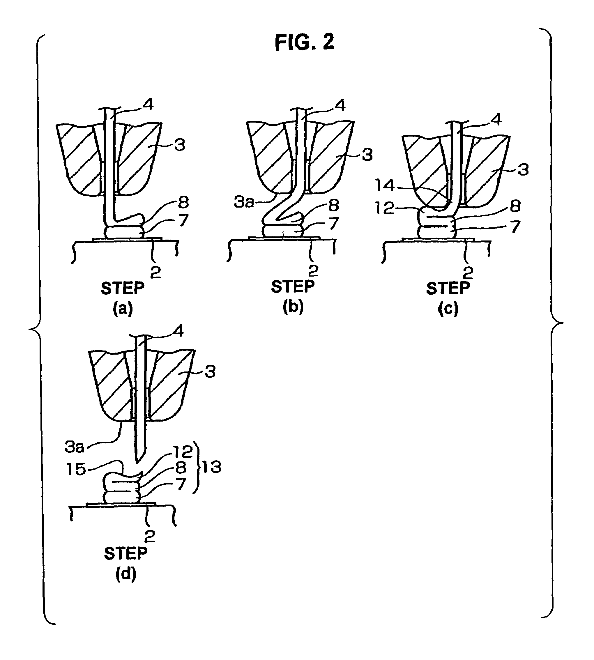
[0032]FIG. 2 shows the present invention.

[0033]This embodiment shows a case in which a three-stage bump 13 is formed (as shown in the illustration for the step (d) in FIG. 2) by forming a third bump 12 which has an inclined wedge 15 formed by the transfer of the external shape of the lower end surface 3a of the capillary 3 on top of the second bump 8 formed in the steps shown in FIG. 1. The step (a) in FIG. 2 is the one that follows the step (g) in FIG. 1.

[0034]Following the step (g) in FIG. 1, the capillary 3 is raised in step (a) of FIG. 2 with the damper (not shown) kept opened.

[0035]In step (b) of FIG. 2, the capillary 3 is moved in the horizontal direction (to the right) so that the flat portion 3a of the capillary 3 is positioned to face the second bump 8.

[0036]Then, in step (c), the capillary 3 is lowered, the wire 4 is bent and pressed while being completely superimposed on the surface of the second bump 8, and ultrasonic waves are applied so that a cut-out 14 is formed. As ...


PUM

PropertyMeasurementUnit
heightaaaaaaaaaa
shapeaaaaaaaaaa
internal diameteraaaaaaaaaa

Abstract

Bump formation method and wire bonding method including a step of forming a ball on the tip end of a wire that passes through a capillary and joining this ball to an electrode pad so as to make a press-bonded ball. In the next step, the capillary is raised and moved horizontally so that the bottom flat portion of the capillary faces the press-bonded ball. Then, the capillary is lowered and the press-bonded ball is pressed, thus forming a first bump. Next, the capillary is raised and moved horizontally in a direction that is opposite from the previous horizontal-direction, thus positioning the flat portion of the capillary to face the first bump. Then, the capillary is lowered, and the wire is bent and pressed against the surface of the first bump so as to form a second bump. The wire is then cut from the second bump.

Description

BACKGROUND OF THE INVENTION[0001]1. Field of the Invention[0002]The present invention relates to a bump formation method for use in the mounting of semiconductor elements, in the connection of wires, etc. and to a wire bonding method for performing wire bonding between two conductors.[0003]2. Prior Art[0004]The method shown in FIG. 5 (see Japanese Patent Application Publication (Kokoku) No. 6-95468 (corresponding to Japanese Patent Application Laid-Open (Kokai) No. 63-304587)) and the method shown in FIG. 6 (see Japanese Patent No. 2735022 (corresponding to Japanese Patent Application Laid-Open (Kokai) No. 8-264540)) are the conventional bump formation methods that allow the formation of bumps with a large height in an extremely simple manner.[0005]In the bump formation method shown in FIG. 5, as seen from the illustration of step (e) in FIG. 5, the bottom portion 20 of a projection-form contact point is formed on top of an electrode pad 2 on the surface of a semiconductor element 1...

Claims


Application Information

Patent Timeline
Patent Type & Authority Patents(United States)
IPC IPC(8): B23K31/02H01L21/60B23K20/00
CPCB23K20/004H01L24/85H01L24/48H01L2924/01033H01L24/78H01L2224/0401H01L2224/05599H01L2224/1134H01L2224/1308H01L2224/48091H01L2224/48227H01L2224/48465H01L2224/48471H01L2224/48479H01L2224/4848H01L2224/48486H01L2224/48487H01L2224/78301H01L2224/85051H01L2224/8518H01L2224/85186H01L2224/85399H01L2224/85986H01L2924/01004H01L2924/01005H01L2924/01006H01L2924/01082H01L2924/00014H01L2224/45099H01L2924/00H01L2224/85045H01L2224/85203H01L2224/85205H01L2924/15787H01L2224/4554A61C8/006A61C8/0068A61C8/0074
Inventor MII, TATSUNARI
Owner SHINKAWA CO LTD
Why Eureka
Try Eureka