Conductive bump, method for forming the same, and electronic component mounting structure using the same

a technology of conductive bumps and bumps, which is applied in the direction of printed circuits, printed electric components, lithography/patterning, etc., can solve the problems of low productivity, complicated bump formation steps, and difficulty in current solder-bump formation technologies to meet such requirements, and achieve low connection resistance, high flatness, and high connection strength

Inactive Publication Date: 2009-12-10
PANASONIC CORP
View PDF3 Cites 23 Cited by
  • Summary
  • Abstract
  • Description
  • Claims
  • Application Information

AI Technical Summary

Benefits of technology

[0021]Thus, it is possible to realize an electronic component mounting structure with high connection strength and low connection resistance in which a semiconductor element with high flatness and a circuit board with high flatness are not needed.

Problems solved by technology

However, it is difficult for current solder-bump formation technologies to meet such requirements.
However, although the plating method is suitable for forming bumps with a narrow pitch, the bump formation step is complicated and the productivity is low.
Meanwhile, although the screen printing method is excellent in productivity, use of a mask makes it difficult to form a bump satisfying a narrow pitch and a high aspect ratio.
In particular, in a semiconductor element including an insulating layer made of a porous and fragile dielectric material, destruction of the insulating layer, cracking of the semiconductor element, and the like, may occur, or the property of the semiconductor element may be changed by stress.
Furthermore, when a semiconductor element having an area bump is mounted, high flatness is required with respect to the entire mounting area of a circuit board.
Furthermore, in general, it is difficult to form conductive bumps having uniform height due to the thermal contraction of the contained resin and the like.
However, in a semiconductor element having a fragile insulating layer with low dielectric constant for increasing the performance, destruction or damage may occur due to press contact at the time of mounting.
Furthermore, it is difficult to maintain the shape of a conductive bump and to realize a stable connection because of press contact with a high pressurizing force.
As a result, in a semiconductor element including a fragile insulating layer, the occurrence of the destruction or damage of the semiconductor element by stress at the time of press contact is further increased.
Furthermore, since the shape of the metal bump is not easily changed, when the semiconductor element is mounted on a wiring board having a low flat accuracy via the metal bump, variation easily occurs in the connection resistance corresponding to the connection area according to the amount of the shape change in the tip portion of the metal bump.

Method used


Image

  • Conductive bump, method for forming the same, and electronic component mounting structure using the same
  • Conductive bump, method for forming the same, and electronic component mounting structure using the same
  • Conductive bump, method for forming the same, and electronic component mounting structure using the same

Examples


first exemplary embodiment

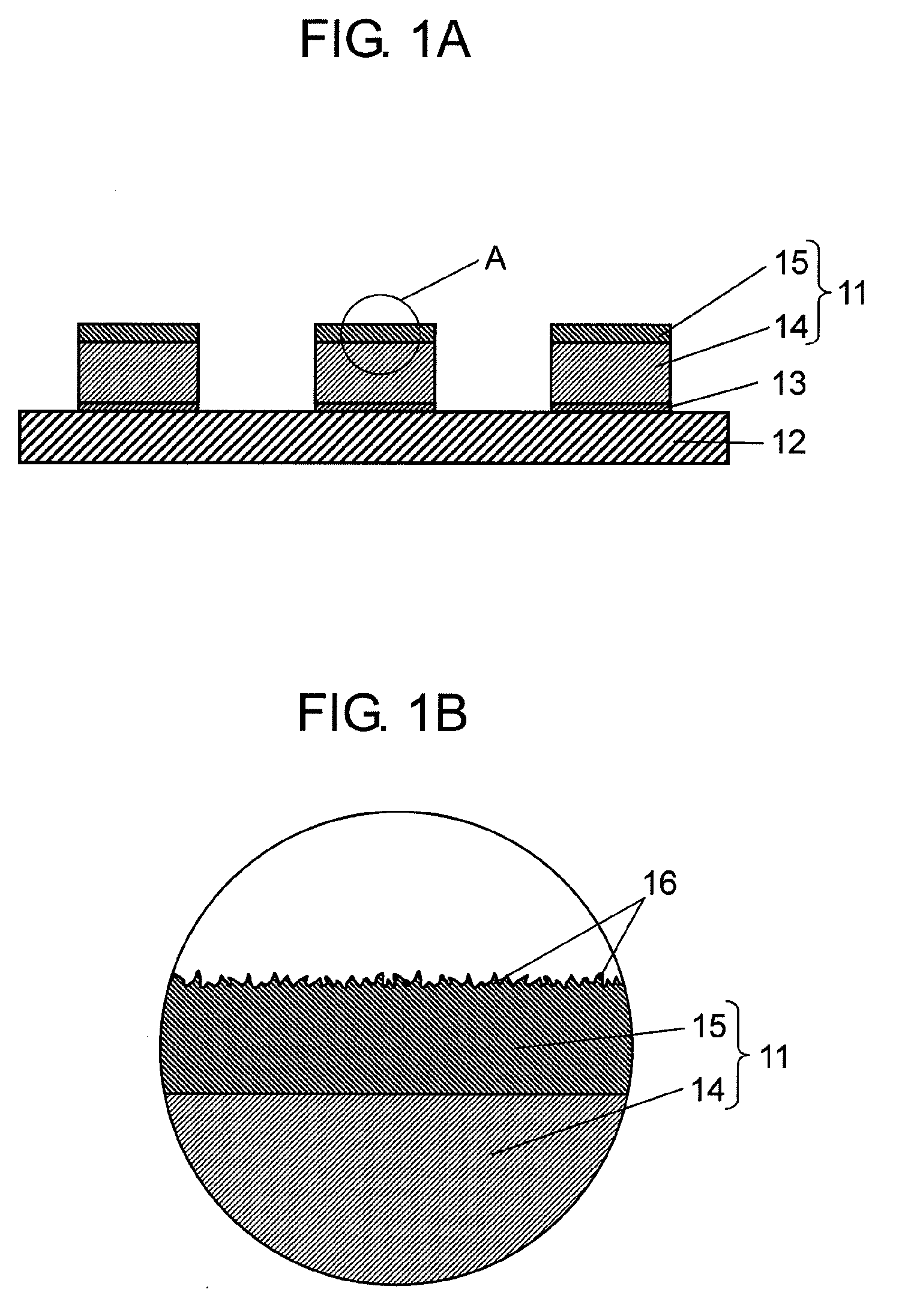
[0055]Hereinafter, with reference to FIGS. 1A and 1B, a structure of a conductive bump of a first exemplary embodiment of the present invention is described. Hereinafter, an example in which a semiconductor element is used as an electronic component and a conductive bump is formed on the semiconductor element is described. However, the same is true in the case in which a circuit board is used.

[0056]Furthermore, an electrode of the electronic component is expressed by using an electrode terminal for the semiconductor element and a connection terminal for the circuit board.

[0057]FIG. 1A is a sectional view illustrating a structure of a conductive bump in accordance with the first exemplary embodiment of the present invention. FIG. 1B is an enlarged sectional view of part A in FIG. 1A.

[0058]As shown in FIG. 1A, conductive bump 11 is provided on each of 100 μm×100 μm electrode terminals 13 disposed with a pitch of, for example, 150 μm on semiconductor element 12 including a semiconducto...

second exemplary embodiment

[0106]Hereinafter, a conductive bump in accordance with a second exemplary embodiment of the present invention is described with reference to FIG. 8.

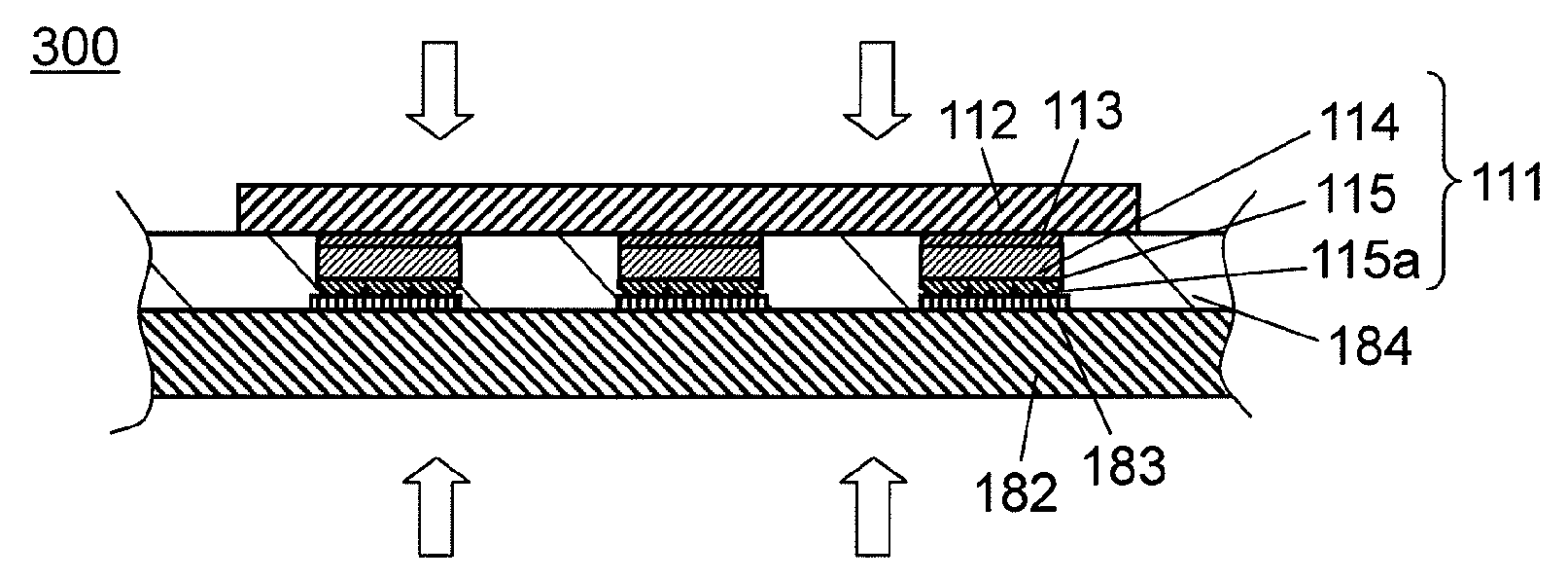
[0107]FIG. 8 is a sectional view illustrating a conductive bump in accordance with the second exemplary embodiment of the present invention. The conductive bump of this exemplary embodiment is different from conductive bump11 of the first exemplary embodiment in that second bump 65 is provided not only on the upper surface of first bump 64 but also on electrode terminal 13 of semiconductor element 12.

[0108]That is to say, as shown in FIG. 8, conductive bump 61 is formed in a state in which first bump 64 including a spherical-shaped conductive filler and photosensitive resin is sandwiched between second bumps 65 including a scale-shaped conductive filler and photosensitive resin. Thus, since the connection resistance of semiconductor element 12 with respect to electrode terminal 13 can be reduced by the scale-shaped conductive filler, co...

third exemplary embodiment

[0129]Hereinafter, a structure of a conductive bump in accordance with a third exemplary embodiment of the present invention is described with reference to FIG. 10. Hereinafter, similar to the first exemplary embodiment, an example in which a semiconductor element is used as an electronic component and a conductive bump is formed on the semiconductor element is described. However, the same is true in the case in which a circuit board is used. Since a configuration of the semiconductor element, a material of conductive filler forming the conductive bump, a shape, and materials of resin or photosensitive resin, and the like, are the same as those in the first exemplary embodiment, the description thereof is omitted herein.

[0130]Furthermore, an electrode of the electronic component is expressed by using an electrode terminal for the semiconductor element and a connection terminal for the circuit board.

[0131]FIG. 10 is a sectional view illustrating a structure of a conductive bump in ac...


PUM

PropertyMeasurementUnit
diameteraaaaaaaaaa
sizeaaaaaaaaaa
sizeaaaaaaaaaa

Abstract

A conductive bump formed on an electrode of an electronic component. The conductive bump is composed of a first bump having one or more layers formed on the electrode and including resin containing at least a spherical-shaped conductive filler, and a second bump formed on an upper surface of the first bump and including photosensitive resin containing a scale-shaped conductive filler.

Description

BACKGROUND OF THE INVENTION[0001]1. Field of the Invention[0002]The present invention relates to a conductive bump formed on an electrode terminal of a semiconductor element or a connection terminal of a circuit board. More particularly, the present invention relates to a conductive bump capable of mounting narrow-pitched electrode terminals of a semiconductor element onto connection terminals of a circuit board with high connection reliability, a method for forming the conductive bump, and an electronic component mounting structure using the conductive bump.[0003]2. Background Art[0004]Recently, in mobile electronic devices such as portable telephones, notebook-sized personal computers and digital video cameras, technology development for realizing small-size and high-performance devices has been rapidly advanced.[0005]One principle electronic component for supporting this technology development is a semiconductor element. In order to realize a thinner and higher-density semiconduc...

Claims


Application Information

Patent Timeline
Patent Type & Authority Applications(United States)
IPC IPC(8): H05K1/16H05K1/11H01R43/02
CPCH01L24/05Y10T29/49213H01L24/13H01L24/29H01L24/32H01L24/90H01L2224/1132H01L2224/114H01L2224/11552H01L2224/11554H01L2224/116H01L2224/11901H01L2224/13016H01L2224/1308H01L2224/13082H01L2224/13083H01L2224/13084H01L2224/1329H01L2224/133H01L2224/16H01L2224/83192H01L2224/90H01L2924/01013H01L2924/01022H01L2924/01029H01L2924/0103H01L2924/01047H01L2924/01049H01L2924/01078H01L2924/01079H01L2924/01082H01L2924/14H05K1/095H05K3/4007H05K2201/0367H05K2201/0373H05K2201/09827H05K2203/0514H05K2203/1476H01L24/11H01L2224/0401H01L2924/014H01L2924/01074H01L2924/01033H01L2924/01024H01L2924/01019H01L2924/01006H01L2924/01005H01L2924/00013H01L2224/05644H01L2224/0558H01L2924/00014H01L2224/13099H01L2924/3512H01L2924/00
Inventor OCHI, SHOZOUSHIROKAWA, KAZUYAHIGUCHI, TAKAYUKI
Owner PANASONIC CORP
Why Eureka
Try Eureka