Switchable band-pass filter

a bandpass filter and switchable technology, applied in waveguide devices, electrical equipment, impedence networks, etc., can solve the problems of large mechanical dimensions, heavy mass, and robustness of filters, and achieve the effect of optimum flatness of filter transmission functions and small space requirements

Active Publication Date: 2012-12-20
ROHDE & SCHWARZ GMBH & CO KG
View PDF7 Cites 10 Cited by
  • Summary
  • Abstract
  • Description
  • Claims
  • Application Information

AI Technical Summary

Benefits of technology

[0011]This direct interaction of the first and second filter element ensures a small structural size of the overall band-pass filter and is achieved through the absence of further conductor elements, possibly connected to earth, between the first and the second filter element. The first and the second filter element are therefore structured directly adjacent to one another although at a distance. The realization of the first and the second filter element in the form of double-circuit resonator filters comprising microstripline technology allows the band-pass filter to be structured using multi-layer printed-circuit board technology and is therefore efficient and can be manufactured at low cost. In this context, the microstriplines are shorted at one end. The small overall mass of the band-pass filter and the distribution of the masses in the band-pass filter according to the invention are particularly suited for use in mobile communications devices. Similarly, the structure comprising microstripline technology allows a low-temperature coefficient without special temperature compensation or adjustment of the filter during operation over a wide temperature range from −30° C. to +80° C.
[0012]In particular, it is advantageous if the coupling device is realized as a network formed from capacitors and / or inductances and semiconductor diodes. In particular, PIN diodes are suitable for semiconductor diodes to be used as switch elements for the transmission of relatively high powers, however, varactor diodes can also be used with relatively low powers.
[0013]A space-saving realization of the band-pass filter on multi-layer printed-circuit boards is particularly preferred, wherein the first and the second filter element can be applied using microstripline technology to one or more layers of the printed-circuit board, and the coupling device is realized on one or more layers. The band-pass filter can also be structured in an appropriate manner so that the input connection of the band-pass filter is formed on an appropriately shaped portion of the first filter element, and the output connection is formed on an appropriately shaped portion of the second filter element. Moreover, in a preferred embodiment of the band-pass filter according to the invention, the coupling network can be formed in such a manner that the capacitors connectable to the first and second filter element are identical in size. This means that the filter can advantageously be operated with identical properties in the forward direction (transmission filter) and in the return direction (reception filter). This presupposes that the first and second filter elements are structured in a symmetrical manner relative to one another. The identity of the resonators can be guaranteed through the use of stripline technology.
[0015]If the band-pass filter is realized in the form of line portions, it is favourable to guide the line portions of the first and the second filter element in such a manner relative to one another that, on the one hand, line portions are disposed parallel to one another in order to achieve a direct coupling between the first and the second filter element in parallel portions, and, furthermore, to keep the space requirement for the filter elements and the band-pass filter as a whole as small as possible.
[0016]In a further, particularly appropriate embodiment of the band-pass filter, the first and the second filter elements comprise mutually parallel line portions, which are arranged in alternation and connected to one another at one end in a conductive manner. It is particularly advantageous if the first and the second filter element are each connected to at least one further line portion, which is formed for the tuning of the respective filter element. Accordingly, an exact calibration of the first and second filter element with reference to their filter mid-frequency is therefore possible in a simple manner, if required. Optimum flatness of the filter transmission function within the passband can be achieved in this manner. A structure of the parallel line portions of the first filter element, on the one hand, and of the second filter element, on the other hand, on different layers of the printed-circuit board is particularly favourable in order to achieve a small space requirement of the band-pass filter and the direct electromagnetic interaction between the first filter element and the second filter element.

Problems solved by technology

The use of two coil resonators leads to large mechanical dimensions, heavy mass, corresponding disadvantages in the robustness of the filter with regard to vibration stress, and large dimensions of the filter component group as a whole.
A filter component group realized on this technical basis leads to correspondingly unfavourable requirements for integration in mobile devices.
Moreover, a band-pass filter with two coil resonators is associated with further disadvantages during manufacture, calibration and operation.
On the one hand, a corresponding filter structure for automated manufacture in production lines designed for surface-mounted components (English: surface mounted devices, abbreviation: SMD) and re-flow soldering methods (English: reflow soldering) is not possible in a fully automated manner, but also requires manual manufacturing steps.
A tuneable band-pass filter realized in this manner is cost intensive to manufacture and structured in a complex manner.

Method used


Image

  • Switchable band-pass filter
  • Switchable band-pass filter
  • Switchable band-pass filter

Examples


Embodiment Construction

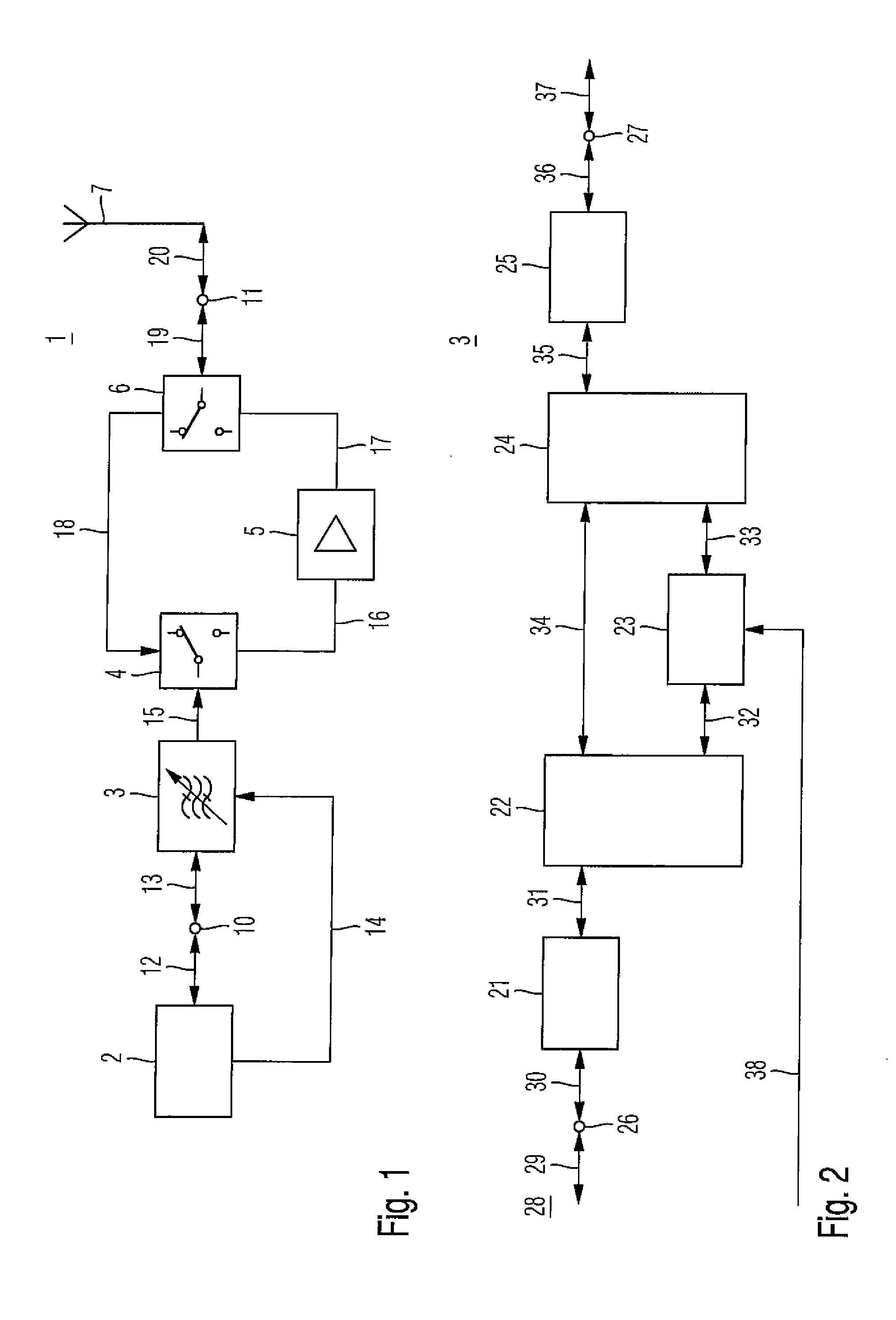
[0028]Before focusing on the structure of the switchable band-pass filter according to the invention, an appropriate application for the filter in a communications device 1 will first be described with reference to FIG. 1. A transceiver 2 is connected via a switchable band-pass filter 3 to an antenna 7. The mid-frequency for the signal 13, 15 to be transmitted or to be received is specified to the switchable band-pass filter 3 via a digital signal 14. The band-pass filter 3 is contained both in the transmission path 12, 13, 15, 16, 17, 19, 20 and also in the reception path 20, 19, 18, 15, 13, 12 of the communications device. Within the transmission path, a power amplifier 5 is additionally connected into the transmission signal path via the switches 4, 6 (realizable, for example, by circulators 4, 6). If the transceiver 2 is operated in frequency-hopping mode (English: frequency hopping), the mid-frequency of the band-pass filter, switched via the digital signal 14 from the transcei...


PUM


Abstract

The invention relates to a switchable band-pass filter. In particular, the invention relates to a narrowband switchable band-pass filter over a broad frequency band with two filter elements (including microstripline technology, suitable for use as a cosite filter with a compact structure, which is particularly suitable for efficient mass production and robust in operation. The two filter elements in this context are coupled to one another, on the one hand via a switchable coupling device and, on the other hand, via a direct electromagnetic interaction.

Description

CROSS-REFERENCE TO RELATED APPLICATION[0001]The present application is a national phase application of PCT Application No. PCT / EP2011 / 000201, filed on Jan. 19, 2011, and claims priority to German Patent Application No. DE 10 2010 008 483.2, filed on Feb. 18, 2010, the entire contents of which are herein incorporated by reference.BACKGROUND OF THE INVENTION[0002]1. Field of the Invention[0003]The invention relates to a switchable band-pass filter. In particular, the invention relates to a narrowband band-pass filter switchable over a broad frequency band with two filter elements comprising microstripline technology, suitable for use as a so-called cosite filter with a compact structure which is particularly suitable for mass production and robust in operation.[0004]2. Discussion of the Background[0005]Frequency-hopping methods are used to an increasing extent in radio communications technology. Accordingly, the carrier frequency of the transmission link alternates in a rapid sequence...

Claims


Application Information

Patent Timeline
Patent Type & Authority Applications(United States)
IPC IPC(8): H01P1/20
CPCH03H7/01H03H7/1766H03H11/04H01P7/088H01P1/2039H01P1/20381H01P1/20345H01P1/20336H01P3/08
Inventor SCHICK, MICHAELKASTE, NORBERT
Owner ROHDE & SCHWARZ GMBH & CO KG
Why Eureka
Try Eureka