Methods and apparatus for performing multiple photoresist layer development and etching processes

Active Publication Date: 2012-12-20
APPLIED MATERIALS INC
View PDF3 Cites 33 Cited by
  • Summary
  • Abstract
  • Description
  • Claims
  • Application Information

AI Technical Summary

Benefits of technology

[0010]The present invention provides methods and an apparatus for controlling and minimizing process defect in a development process, and modifying LWR of a photoresist layer after the development process. In one embodiment, a method for forming features on a substrate includes generating an electric field in a processing chamber having a substrate disposed therein, wherein the substrate has a photosensitive layer having exposed areas and non-exposed areas, supplying a first gas mixture into the processing cha

Problems solved by technology

Integrated circuits have evolved into complex devices that can include millions of components (e.g., transistors, capacitors and resistors) on a single chip.
Accordingly, lithography processes have become more and more challenging to transfer even smaller features onto a substrate precisely and accurately without damage.
However, at such small dimensions, the roughness of the edges of a photoresist layer has become harder and harder to control.
As the feature sizes formed on microelectronic devices continue to shrink, the aqueous base solution developer may become problematic due to image collapse caused by the capillary forces and surface tension of water.
Furthermore, solution based developer tends to leave undesired contaminates on the substrate after the deve

Method used


Image

  • Methods and apparatus for performing multiple photoresist layer development and etching processes
  • Methods and apparatus for performing multiple photoresist layer development and etching processes
  • Methods and apparatus for performing multiple photoresist layer development and etching processes

Examples


Example

[0022]To facilitate understanding, identical reference numerals have been used, where possible, to designate identical elements that are common to the figures. It is contemplated that elements and features of one embodiment may be beneficially incorporated in other embodiments without further recitation.

[0023]It is to be noted, however, that the appended drawings illustrate only exemplary embodiments of this invention and are therefore not to be considered limiting of its scope, for the invention may admit to other equally effective embodiments.

DETAILED DESCRIPTION

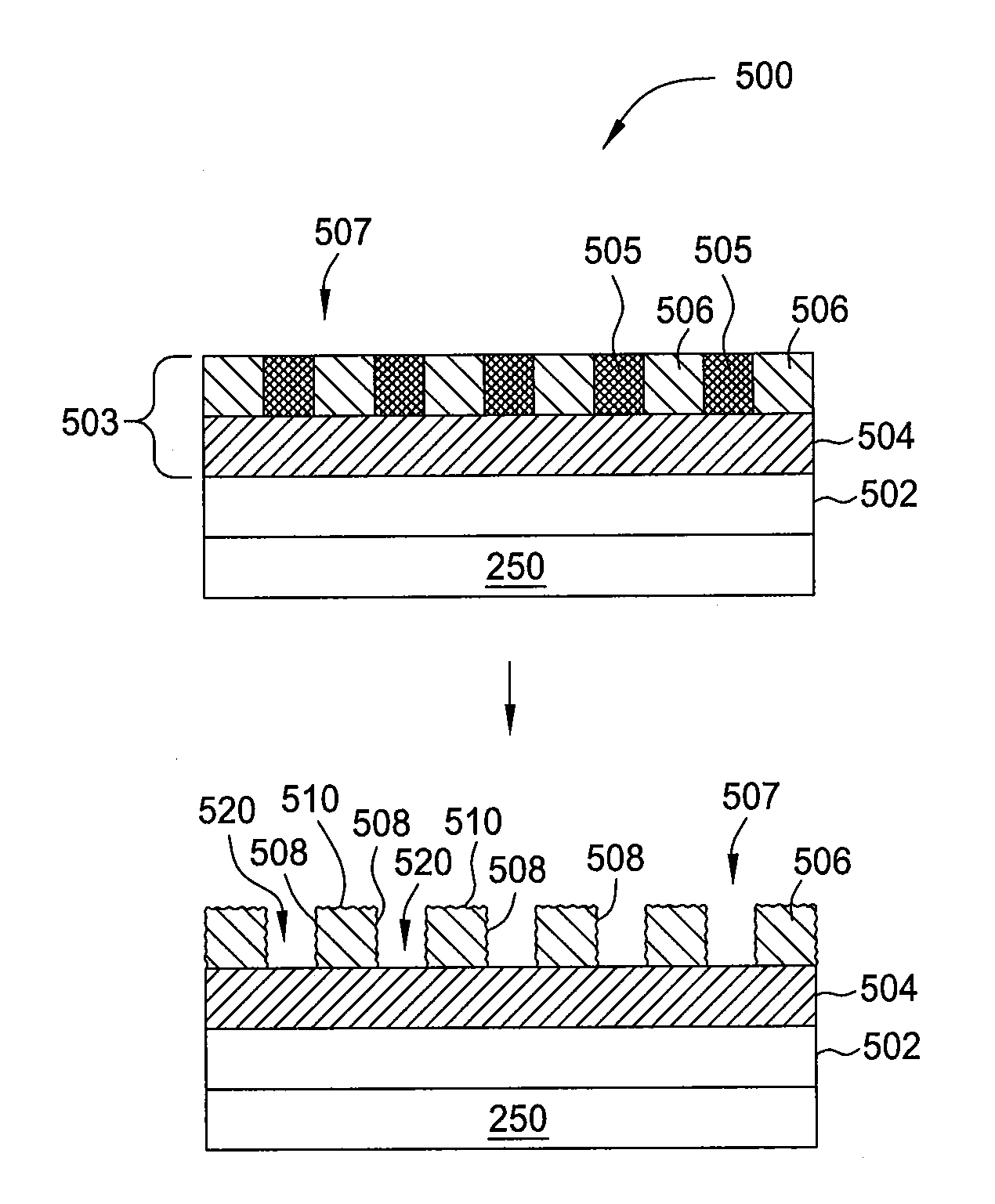
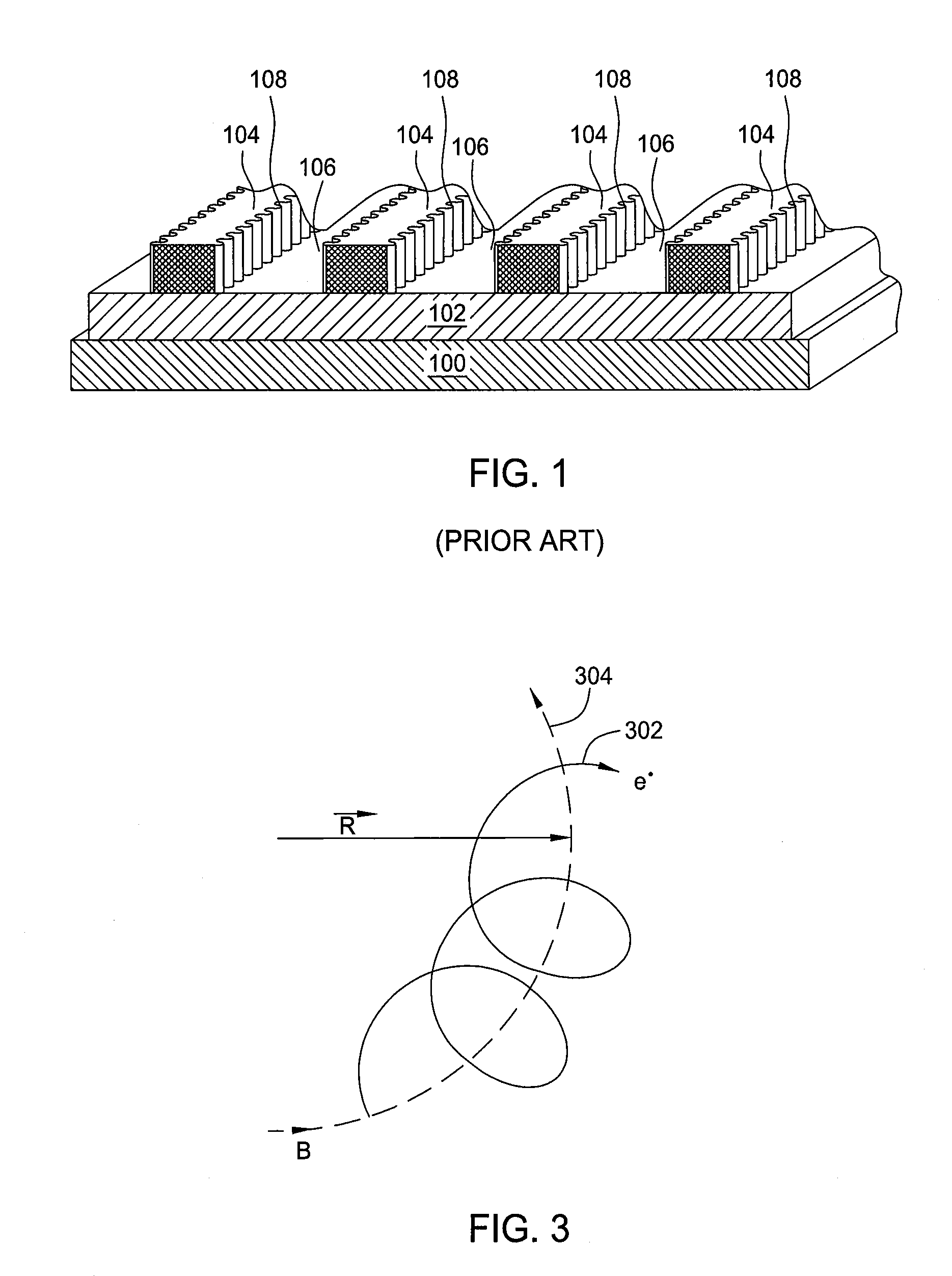
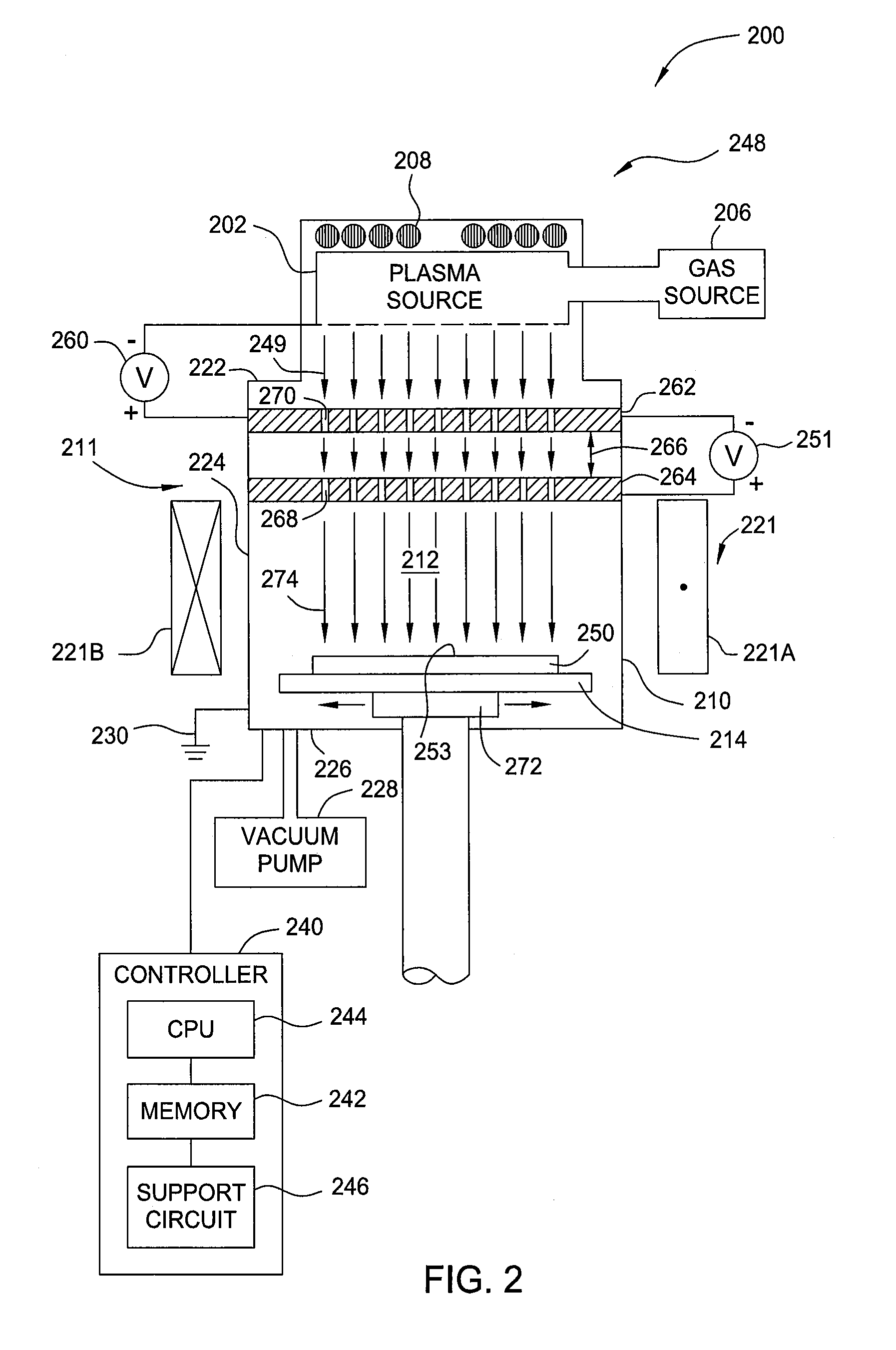
[0024]Embodiments of the present invention include methods and apparatus for controlling and minimizing process defect in a development process, modifying LWR of a photoresist layer after the development process, and maintaining good profile control during subsequent etching processes. The development process may be performed in an inductively coupled plasma (ICP) reactor to dry plasma develop the photoresist layer after a...


PUM


Abstract

The present invention provides methods and an apparatus controlling and minimizing process defects in a development process, and modifying line width roughness (LWR) of a photoresist layer after the development process, and maintaining good profile control during subsequent etching processes. In one embodiment, a method for forming features on a substrate includes developing and removing exposed areas in the photosensitive layer disposed on the substrate in the electron processing chamber by predominantly using electrons, removing contaminants from the substrate by predominantly using electrons, and etching the non-photosensitive polymer layer exposed by the developed photosensitive layer in the electron processing chamber by predominantly using electrons.

Description

CROSS REFERENCE TO RELATED APPLICATION[0001]This application claims benefit of U.S. Provisional Patent Application No. 61 / 497,346, filed Jun. 15, 2011, which is incorporated by reference in its entirety.BACKGROUND[0002]1. Field of the Invention[0003]The present invention generally relates to methods and apparatus for performing a photoresist development process, a photoresist line width roughness process, a defect control process, and an etching process and, more specifically, to methods and apparatus for performing a photoresist development process, a photoresist line width roughness process, a defect control process, and an etching process in a single chamber in semiconductor processing technologies.[0004]2. Description of the Related Art[0005]Integrated circuits have evolved into complex devices that can include millions of components (e.g., transistors, capacitors and resistors) on a single chip. The evolution of chip designs continually requires faster circuitry and greater cir...

Claims


Application Information

Patent Timeline
IPC IPC(8): G03F7/36
CPCG03F7/36G03F7/40
Inventor WU, BANQIUKUMAR, AJAYRAMASWAMY, KARTIKNALAMASU, OMKARAM
Owner APPLIED MATERIALS INC
Why Eureka
Try Eureka