Pixel, pixel array, image sensor including the same, method for operating the image sensor

Active Publication Date: 2012-12-27
LG INNOTEK CO LTD
View PDF5 Cites 4 Cited by
  • Summary
  • Abstract
  • Description
  • Claims
  • Application Information

AI Technical Summary

Benefits of technology

[0010]As described above, lights having different wavelength bands, such as infrared wavelengths bands and visible wavelength bands

Problems solved by technology

This is because it is difficult for an image sensor employing a silicon substrate to process mixed image signals obtained from both visible lights and infrared lights.
However, the technology of inserting the layer to transmit only the infrared

Method used


Image

  • Pixel, pixel array, image sensor including the same, method for operating the image sensor
  • Pixel, pixel array, image sensor including the same, method for operating the image sensor
  • Pixel, pixel array, image sensor including the same, method for operating the image sensor

Examples


Example

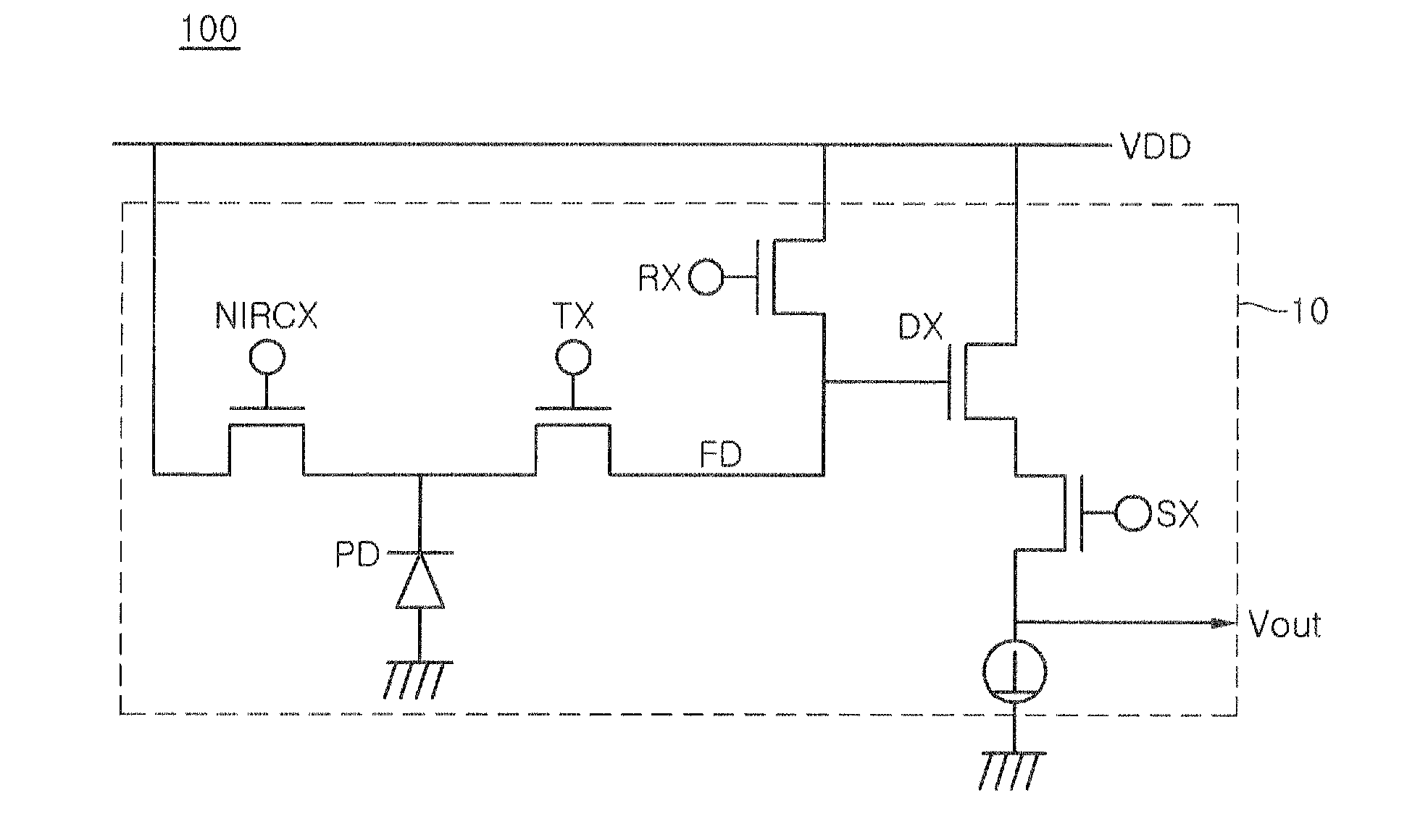
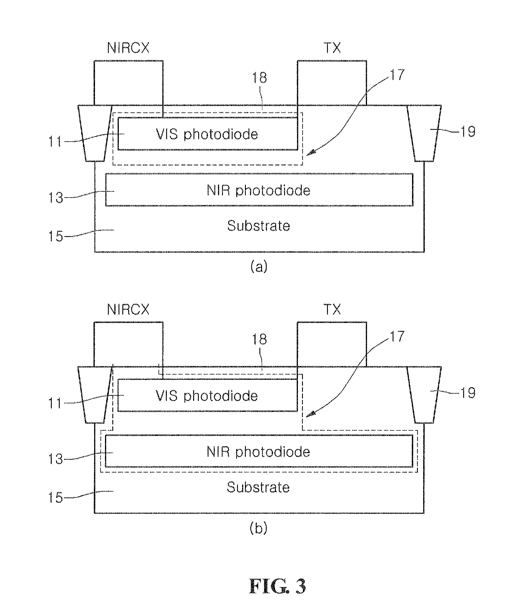
[0017]In the description of the embodiments, it will be understood that, when a layer (or film), a region, a pattern, or a structure is referred to as being “on” or “under” another substrate, another layer (or film), another region, another pad, or another pattern, it can be “directly” or “indirectly” over the other substrate, layer (or film), region, pad, or pattern, or one or more intervening layers may also be present. Such a position of the layer has been described with reference to the drawings.

[0018]The thickness and size of each layer shown in the drawings may be exaggerated, omitted or schematically drawn for the purpose of convenience or clarity. In addition, the size of elements does not utterly reflect an actual size.

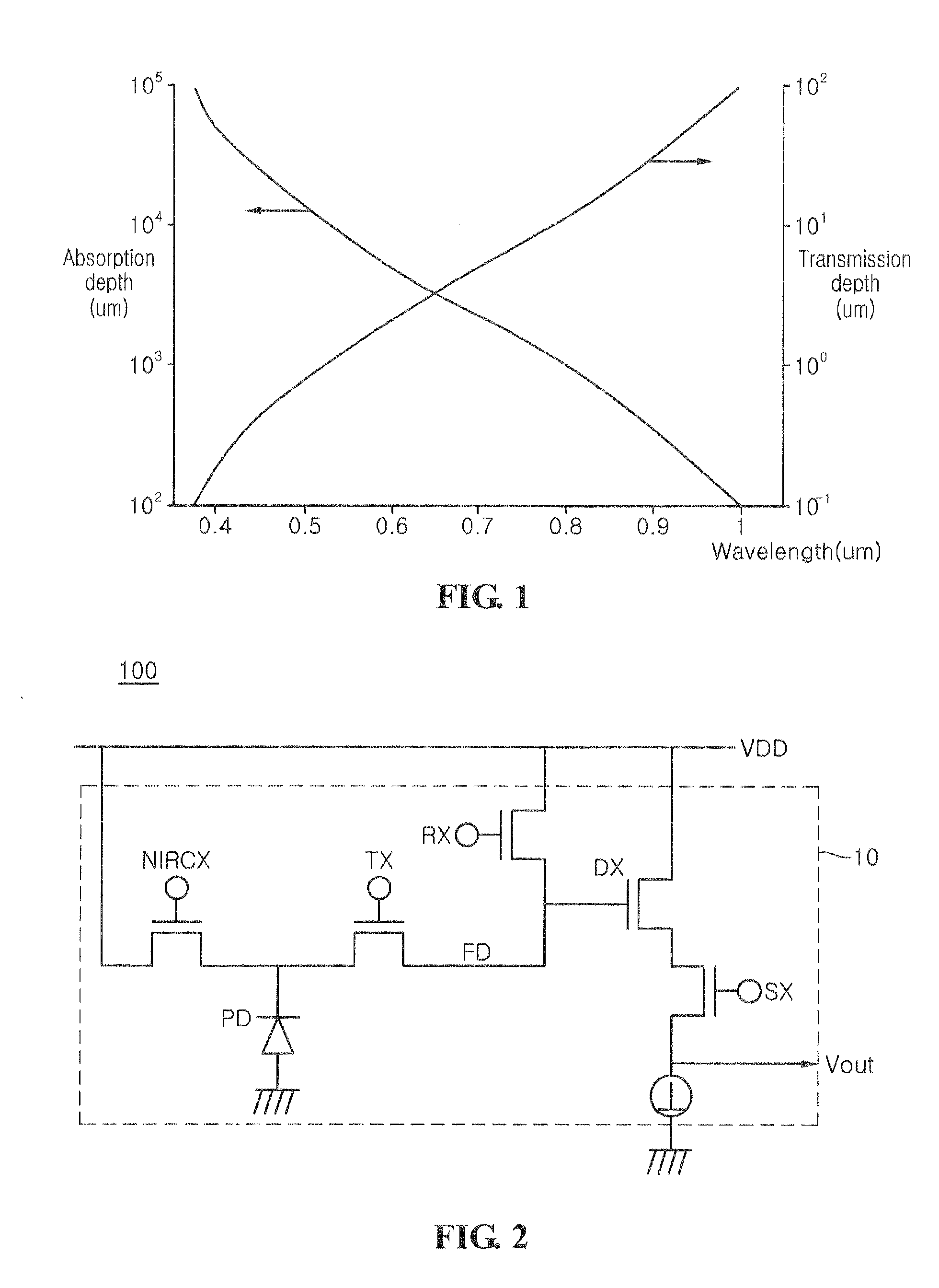
[0019]FIG. 1 is a graph showing the absorption depth and the transmission depth according to wavelengths in a semiconductor substrate. As shown in FIG. 1, the semiconductor substrate onto which a light is incident may be a silicon substrate used for an image ...


PUM


Abstract

Disclosed are a pixel, a pixel array, an image sensor including the same, and a method for operating the image sensor. Charges are eliminated from a first photoelectric conversion region of a photoelectric conversion section, and accumulated into the first photoelectric conversion region. Information about quantity of the charges of the first photoelectric conversion region is output, and charges are removed from a second photoelectric conversion region of the photoelectric conversion section. Accumulation of charges into the second photoelectric conversion region is started, and then information about quantity of the charges accumulated in the second photoelectric conversion region is output.
Lights having wavelength bands different from each other are independently detected according to disclosed invention.

Description

CROSS-REFERENCE TO RELATED APPLICATION[0001]This application claims the benefit under 35 U.S.C. §119 of Korean Patent Application No. 10-2011-0061631, filed on Jun. 24, 2011, which is hereby incorporated by reference in its entirety.BACKGROUND[0002]The embodiment relates to a pixel capable of individually distinguishing between visible and non-visible wavelength bands, a pixel array, an image sensor including the same, and a method for operating the image sensor. In particularly, the embodiment relates to a pixel capable of more simply distinguishing between lights having wavelength bands different from each other to detect the lights by additionally arranging a potential control switching section at one side of a photodiode.[0003]Conventionally, an IR cut filter has been used in a camera module to filter lights having infrared wavelength bands, thereby sensing only lights in visible wavelength bands, so that image processing can be clearly performed. This is because it is difficult...

Claims


Application Information

Patent Timeline
IPC IPC(8): H01L27/146G01J5/10G01J1/44
CPCG01J1/44H01L27/14645H01L27/14609G01J5/20H01L27/14625H04N25/00
Inventor SA, SEUNG HOON
Owner LG INNOTEK CO LTD
Why Eureka
Try Eureka