LOW k POROUS SiCOH DIELECTRIC AND INTEGRATION WITH POST FILM FORMATION TREATMENT

a technology of low k porous sicoh and film formation treatment, applied in the direction of semiconductor/solid-state device details, coatings, chemical vapor deposition coatings, etc., can solve the problems of increasing the stress and crack velocity of the film to levels which are not acceptable, increasing the signal delay of ulsi electronic devices, etc., to reduce the stress change caused by increased tetrahedral strain, less si—o—si bonding, and hydrophobicity improvemen

Active Publication Date: 2012-12-27
TAIWAN SEMICON MFG CO LTD
View PDF19 Cites 21 Cited by
  • Summary
  • Abstract
  • Description
  • Claims
  • Application Information

AI Technical Summary

Benefits of technology

[0016]The present invention also provides a method of forming such a p-SiCOH dielectric film. In particular, the applicants have determined that one can reduce or minimize the stress change and make the p-SiCOH dielectric film more stable and more hydrophobic by selecting an appropriate annealing ambient that has the ability to reduce oxidation of the dielectric film and thus minimize or reduce the formation of Si—OH (and to a lesser extent Si—H) groups on the surface of the dielectric film. In the present invention it has been determined that by annealing in an ambient that includes a gas that contains at least one C—C double bond, at least one C—C triple bond or a combination of at least one C—C double bond and at least one C—C triple bond produces the inventive p-SiCOH dielectric film. In particular, the bonding formation utilizing such an ambient gas produces flexible and stabilized crosslinking —(CHx)— chains at least within the pores of the SiCOH dielectric film. Subsequently, the film stress will be reduced and the film's stability will be improved. The presence of the at least one C—C double bond and / or the at least one C—C triple bond in the annealing ambient also minimizes the impact of residual oxygen in the ambient during annealing and reduces / eliminates the formation of Si—OH and / or Si—H bonding on the surface of the dielectric film forming various bridging bonds.
[0025]The annealing step of the present invention reduces both Si—OH and Si—H bond formation within the pores and on the surface of the p-SiCOH film, increases the film's hydrophobicity, enhances the films stability and reduces the film's stress by reducing the formation of Si—O—Si crosslinking bonds.

Problems solved by technology

This combined effect increases signal delays in ULSI electronic devices.
The formation of Si—O—Si bonds, in turn, increases the film's stress and crack velocity to levels which are not acceptable in semiconductor interconnect structures.

Method used


Image

  • LOW k POROUS SiCOH DIELECTRIC AND INTEGRATION WITH POST FILM FORMATION TREATMENT
  • LOW k POROUS SiCOH DIELECTRIC AND INTEGRATION WITH POST FILM FORMATION TREATMENT
  • LOW k POROUS SiCOH DIELECTRIC AND INTEGRATION WITH POST FILM FORMATION TREATMENT

Examples


Embodiment Construction

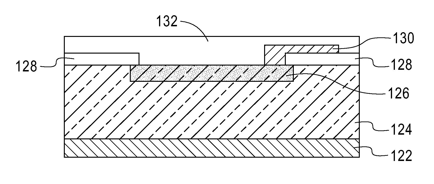
[0039]The present invention, which describes a p-SiCOH dielectric film having a reduced content of Si—OH and Si—H bondings, and increased —(CHx)— bondings within the pores and on the surface of the film, a method of fabricating the same and electronic structures containing the inventive p-SiCOH dielectric film, will now be described in greater detail.

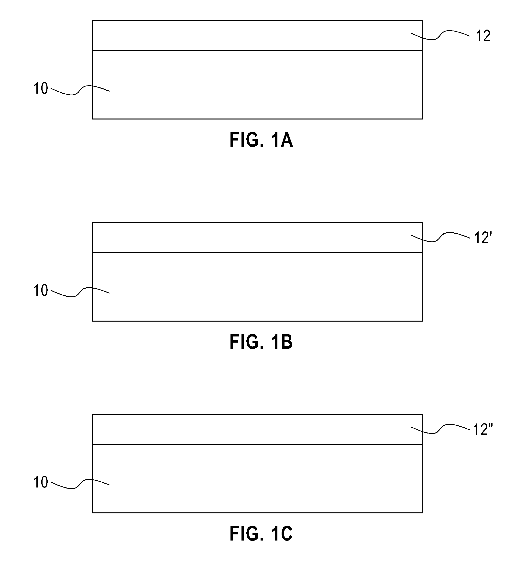
[0040]In accordance with the method of the present invention, a SiCOH dielectric film 12 is formed on a surface of a substrate 10 such as shown, for example, in FIG. 1A. The term “substrate” when used in conjunction with substrate 10 includes, a semiconducting material, an insulating material, a conductive material or any combination thereof, including multilayered structures. Thus, for example, substrate 10 may be a semiconducting material such as Si, SiGe, SiGeC, SiC, GaAs, InAs, InP and other III / V or II / VI compound semiconductors. The semiconductor substrate 10 may also include a layered substrate such as, for example, Si / SiGe, Si / S...


PUM

PropertyMeasurementUnit
dielectric constantaaaaaaaaaa

Abstract

A porous SiCOH dielectric film in which the stress change caused by increased tetrahedral strain is minimized by post treatment in unsaturated Hydrocarbon ambient. The p-SiCOH dielectric film has more —(CHx) and less Si—O—H and Si—H bonding moieties. Moreover, a stable pSiOCH dielectric film is provided in which the amount of Si—OH (silanol) and Si—H groups at least within the pores has been reduced by about 90% or less by the post treatment. A p-SiCOH dielectric film is produced that is flexible since the pores include stabilized crosslinking —(CHx)— chains wherein x is 1, 2 or 3 therein. The dielectric film is produced utilizing an annealing step subsequent deposition that includes a gaseous ambient that includes at least one C—C double bond and / or at least one C—C triple bond.

Description

CROSS REFERENCE TO RELATED APPLICATIONS[0001]This application is a divisional of U.S. patent application Ser. No. 11 / 846,250, filed Aug. 28, 2007, the entire content and disclosure of which is incorporated herein by reference. This application is also related to U.S. Ser. No. 11 / 846,182, (Attorney docket YOR920060748US1; SSMP 20357-1), which cross referenced application was filed on the same date as the parent application, namely, U.S. patent application Ser. No. 11 / 846,250.FIELD OF THE INVENTION[0002]The present invention relates to a semiconductor dielectric film as well as a method of fabricating such a film. More particularly, the present invention relates to a porous dielectric material comprising atoms of at least Si, C, O and H (hereinafter p-SiCOH dielectric) which has a low dielectric constant (k of about 2.7 or less), enhanced post processing stability and improved film properties as compared with prior art p-SiCOH dielectrics. The present invention also relates to a metho...

Claims


Application Information

Patent Timeline
Patent Type & Authority Applications(United States)
IPC IPC(8): H01L21/312
CPCC23C16/401H01L23/53295C23C16/56H01L21/02126H01L21/02203H01L21/02205H01L21/02216H01L21/02274H01L21/0234H01L21/02345H01L21/02348H01L21/02351H01L21/31633H01L21/31695H01L21/76825H01L21/76826H01L21/76828H01L23/5329C23C16/505H01L2924/0002H01L2924/00C23C16/511H01J2237/336H01J2237/338H01J2237/3382
Inventor GATES, STEPHEN M.GRILL, ALFREDNGUYEN, SONNITTA, SATYANARAYANA V.SHAW, THOMAS M.
Owner TAIWAN SEMICON MFG CO LTD
Why Eureka
Try Eureka