LOW k POROUS SiCOH DIELECTRIC AND INTEGRATION WITH POST FILM FORMATION TREATMENT

Inactive Publication Date: 2009-03-05
GLOBALFOUNDRIES INC
View PDF51 Cites 12 Cited by
  • Summary
  • Abstract
  • Description
  • Claims
  • Application Information

AI Technical Summary

Benefits of technology

[0011]The present invention provides a porous SiCOH (p-SiCOH) dielectric film in which the stress change caused by increased tetrahedral strain is minimized. In other terms, the inventive porous SiCOH dielectric film has less Si—O—Si bonding as compared to prior art p-SiCOH dielectric films. Moreover, a stable p-SiOCH dielectric film is provided in which the amount of Si—OH (silanol) and/or Si—H grou

Problems solved by technology

This combined effect increases signal delays in ULSI electronic devices.
The formation of Si—O—Si bonds, in turn, incre

Method used


Image

  • LOW k POROUS SiCOH DIELECTRIC AND INTEGRATION WITH POST FILM FORMATION TREATMENT
  • LOW k POROUS SiCOH DIELECTRIC AND INTEGRATION WITH POST FILM FORMATION TREATMENT
  • LOW k POROUS SiCOH DIELECTRIC AND INTEGRATION WITH POST FILM FORMATION TREATMENT

Examples


Embodiment Construction

[0039]The present invention, which describes a p-SiCOH dielectric film having a reduced content of Si—OH and Si—H bondings, and increased —(CHx)— bondings within the pores and on the surface of the film, a method of fabricating the same and electronic structures containing the inventive p-SiCOH dielectric film, will now be described in greater detail.

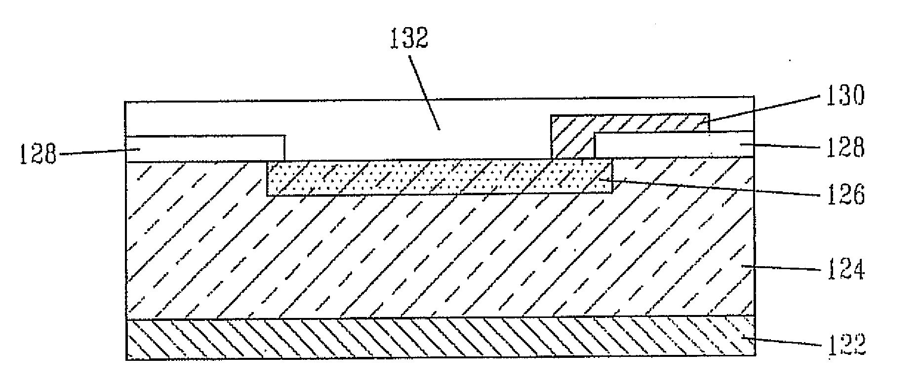
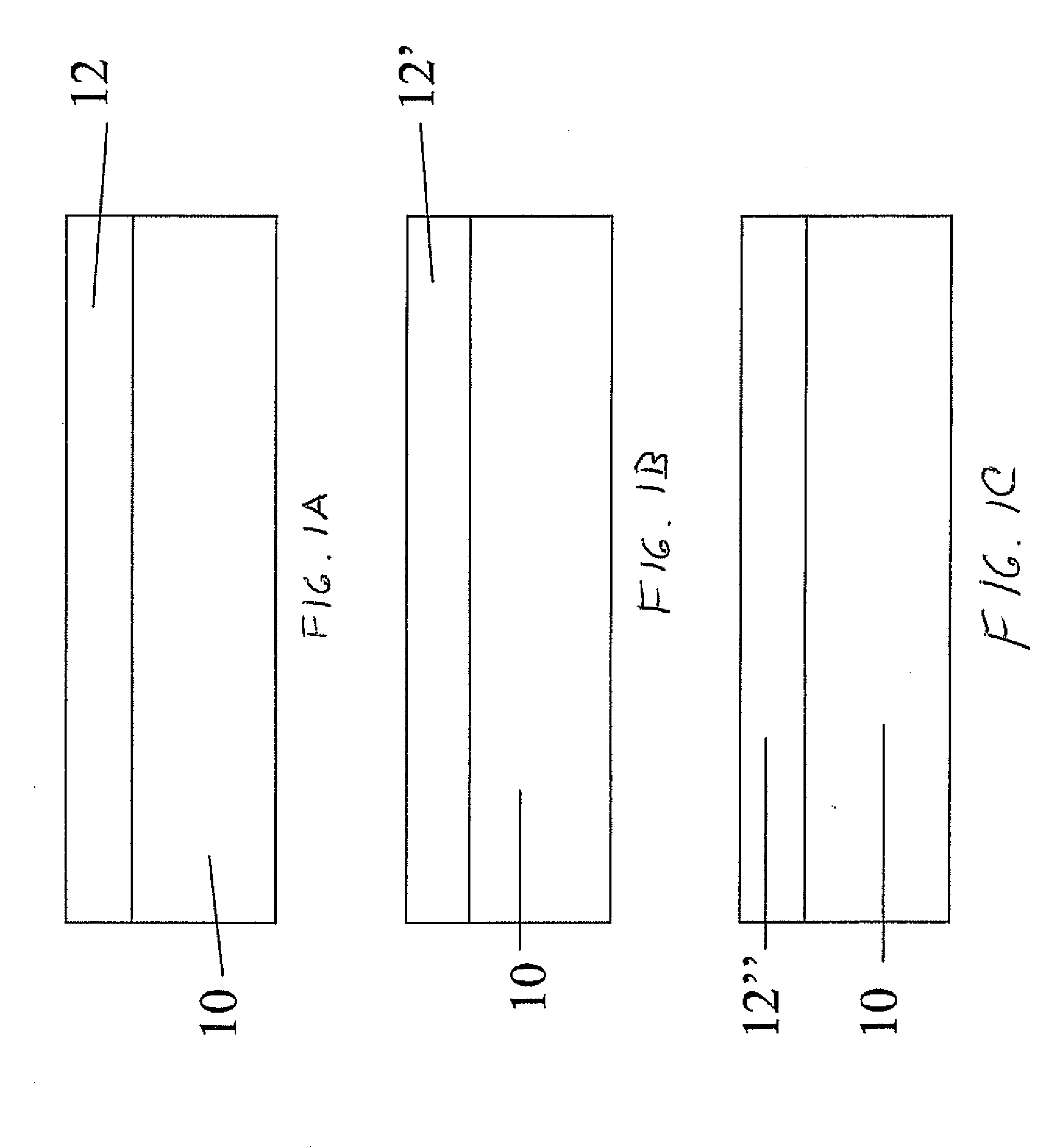
[0040]In accordance with the method of the present invention, a SiCOH dielectric film 12 is formed on a surface of a substrate 10 such as shown, for example, in FIG. 1A. The term “substrate” when used in conjunction with substrate 10 includes, a semiconducting material, an insulating material, a conductive material or any combination thereof, including multilayered structures. Thus, for example, substrate 10 may be a semiconducting material such as Si, SiGe, SiGeC, SiC, GaAs, InAs, InP and other III / V or III / VI compound semiconductors. The semiconductor substrate 10 may also include a layered substrate such as, for example, Si / SiGe, Si / ...


PUM

PropertyMeasurementUnit
Fractionaaaaaaaaaa
Dielectric polarization enthalpyaaaaaaaaaa
Flexibilityaaaaaaaaaa

Abstract

A porous SiCOH (e.g., p-SiCOH) dielectric film in which the stress change caused by increased tetrahedral strain is minimized by post treatment in unsaturated Hydrocarbon ambient. The inventive p-SiCOH dielectric film has more —(CHx) and less Si—O—H and Si—H bondings as compared to prior art p-SiCOH dielectric films. Moreover, a stable pSiOCH dielectric film is provided in which the amount of Si—OH (silanol) and Si—H groups at least within the pores has been reduced by about 90% or less by the post treatment. Hence, the inventive p-SiCOH dielectric film has hydrophobicity improvement as compared with prior art p-SiCOH dielectric films. In the present invention, a p-SiCOH dielectric film is produced that is flexible since the pores of the inventive film include stabilized crosslinking —(CHx)— chains wherein x is 1, 2 or 3 therein. The dielectric film is produced utilizing an annealing step subsequent deposition that includes a gaseous ambient that includes at least one C—C double bond and/or at least one C—C triple bond.

Description

RELATED APPLICATIONS[0001]This application is related to U.S. Ser. No. ______, (Attorney docket YOR920060748US1; SSMP 20357-1), which cross referenced application is being filed concurrently on the same date as the present application.FIELD OF THE INVENTION[0002]The present invention relates to a semiconductor dielectric film as well as a method of fabricating such a film. More particularly, the present invention relates to a porous dielectric material comprising atoms of at least Si, C, O and H (hereinafter p-SiCOH dielectric) which has a low dielectric constant (k of about 2.7 or less), enhanced post processing stability and improved film properties as compared with prior art p-SiCOH dielectrics. The present invention also relates to a method of fabricating such a p-SiCOH dielectric as well as the use of the same as a dielectric in various semiconductor structures, including, for example, interconnect structures.BACKGROUND OF THE INVENTION[0003]The continuous shrinking in dimensio...

Claims


Application Information

Patent Timeline
IPC IPC(8): H01L21/47
CPCC23C16/401H01L23/53295C23C16/56H01L21/02126H01L21/02203H01L21/02205H01L21/02216H01L21/02274H01L21/0234H01L21/02345H01L21/02348H01L21/02351H01L21/31633H01L21/31695H01L21/76825H01L21/76826H01L21/76828H01L23/5329C23C16/505H01L2924/0002H01L2924/00C23C16/511H01J2237/336H01J2237/338H01J2237/3382
Inventor GATES, STEPHEN M.GRILL, ALFREDNGUYEN, SONNITTA, SATYANARAYANA V.SHAW, THOMAS M.
Owner GLOBALFOUNDRIES INC
Why Eureka
Try Eureka