System for display images

a system and image technology, applied in non-linear optics, instruments, optics, etc., can solve the problems of poor adhesion poor bonding between the cf substrate and the planarization layer, and easy peeling between the planarization layer and the metal line of the scan line and the data line. , to achieve the effect of improving the bonding force, preventing the manufacture of conventional liquid crystal display

Inactive Publication Date: 2013-01-03
INNOLUX CORP +1
View PDF1 Cites 46 Cited by
  • Summary
  • Abstract
  • Description
  • Claims
  • Application Information

AI Technical Summary

Benefits of technology

[0007]Accordingly, embodiments of the invention provide a system for displaying images including a display panel. The display panel has a patterned planarization layer which improves a bonding force between two substrates of the display panel. Thus, the peeling issue found in the manufacturing of conventional liquid crystal display panels is prevented from occurring. Further, the yield of the liquid crystal display panels is enhanced.

Problems solved by technology

The adhesion between a material of the planarization layer and a metal material used for the scan lines and the data lines and the adhesion between a material of the planarization layer and an inorganic material used for the TFTs, such as silicon oxide or silicon nitride are poor.
Thus, peeling easily occurs between the planarization layer and the metal lines of the scan lines and the data lines, and between the planarization layer and the inorganic material of the TFTs.
If so, then, there is poor bonding between the CF substrate and the array substrate, which may lead to the separation of the CF substrate and the array substrate.
Therefore, the yield of the conventional liquid crystal display panels is poor.

Method used


Image

  • System for display images
  • System for display images
  • System for display images

Examples


Embodiment Construction

[0016]The description is provided for illustrating the general principles of the invention and is not meant to be limiting. The scope of the invention is best determined by reference to the appended claims.

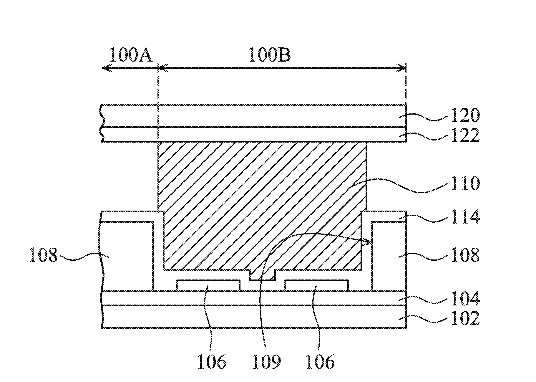
[0017]In embodiments of the invention, a patterned planarization layer is formed on a substrate of a display panel. The patterned planarization layer is disposed between a seal and a metal layer and an insulating layer formed on the substrate. A contact area between the seal and the metal layer and the insulating layer is increased through the design of the patterned planarization layer. Thus, a bonding force between two substrates of the display panel is enhanced to prevent the peeling issue found in the manufacturing of conventional liquid crystal display panels from occurring.

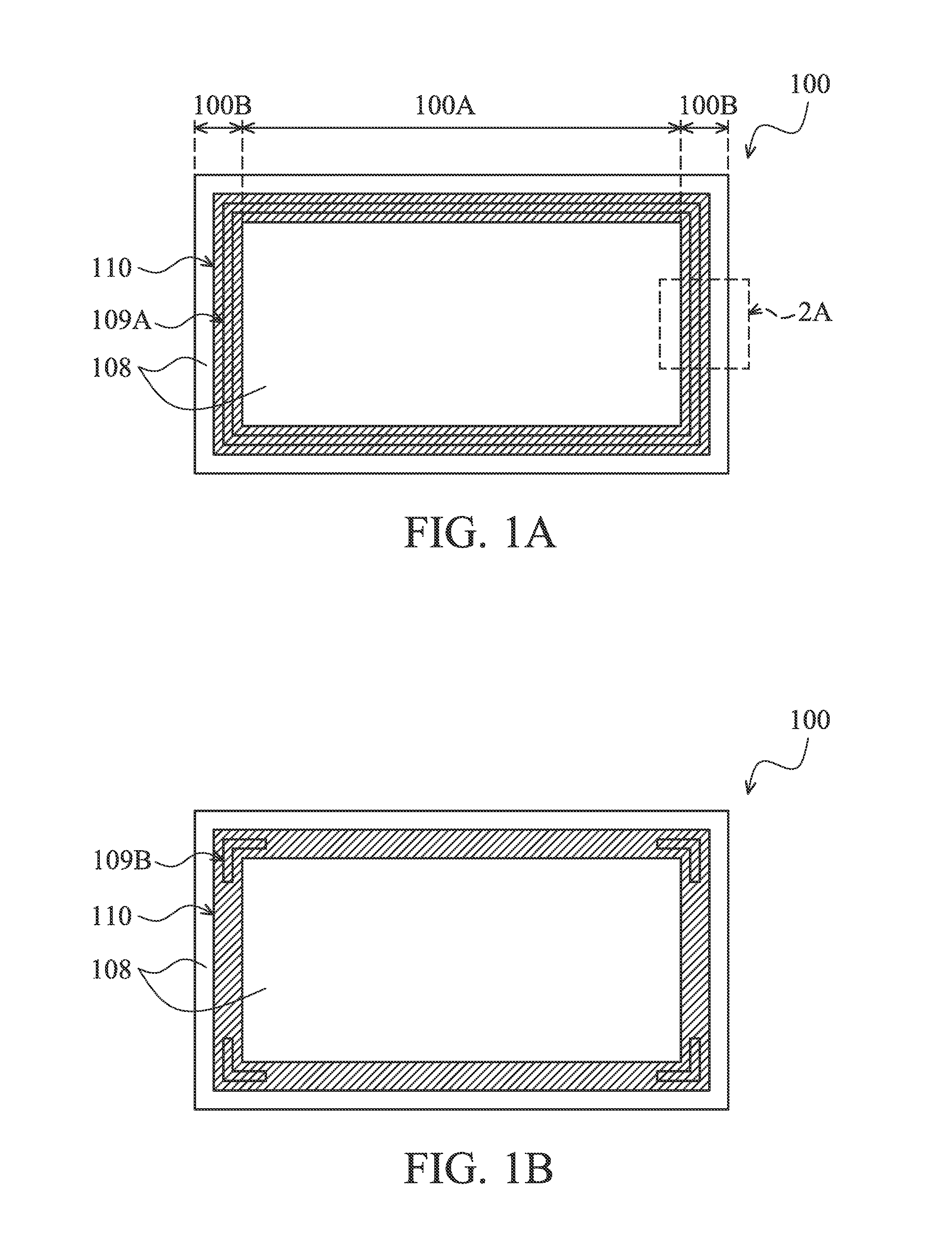
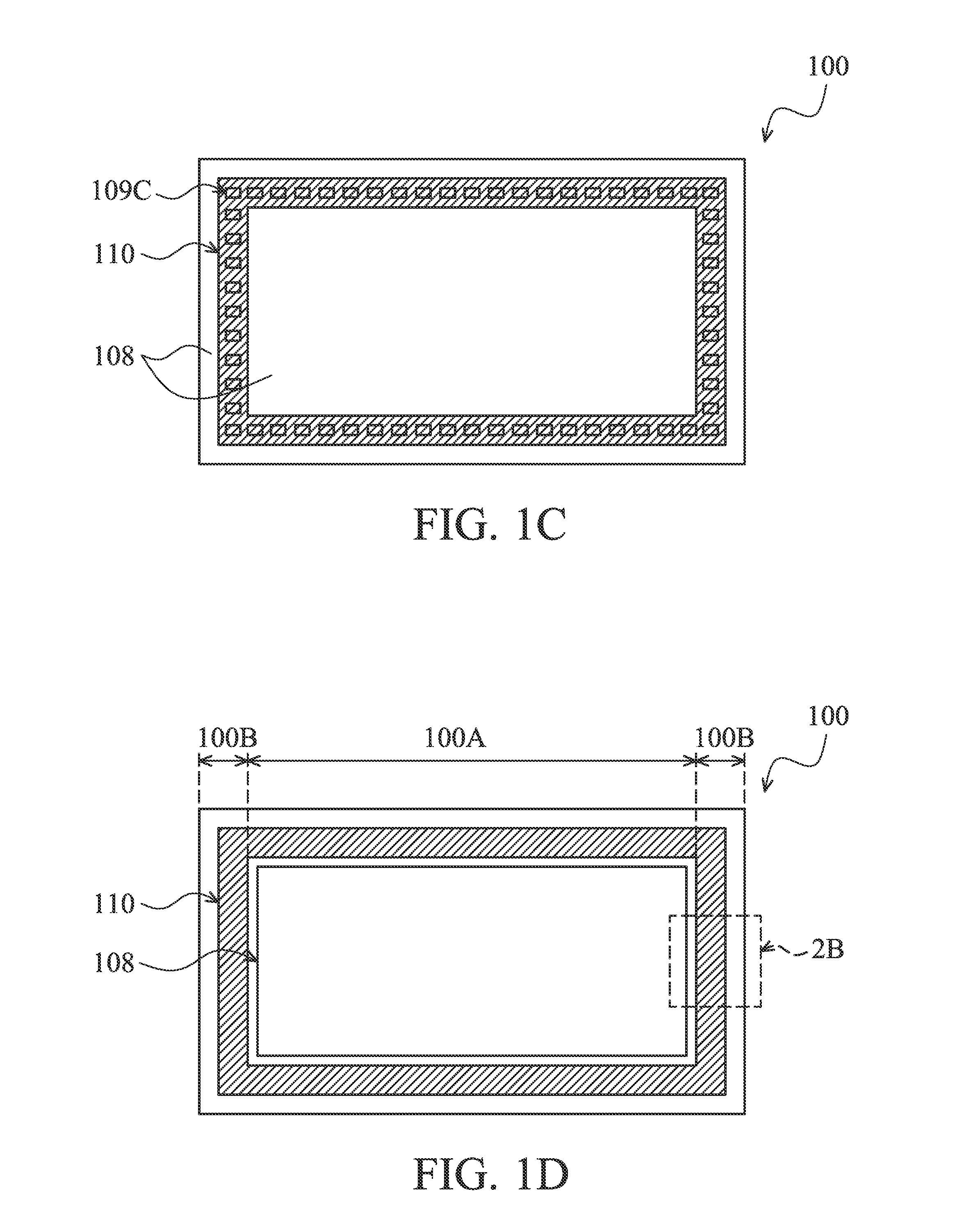
[0018]Referring to FIG. 1A, a plane view of a display panel 100 according to an embodiment of the invention is shown. The display panel 100 has a display area 100A and a peripheral area 100B surrounding th...


PUM

PropertyMeasurementUnit
areaaaaaaaaaaa
adhesionaaaaaaaaaa
bonding forceaaaaaaaaaa

Abstract

A system for displaying images including a display panel is provided. The display panel has a display area and a peripheral area. The display panel includes a metal layer disposed on a first substrate. A patterned planarization layer is disposed on the metal layer, having at least one opening corresponding to the peripheral area, wherein a portion of the metal layer is exposed through the opening. A second substrate is disposed opposite to the first substrate. A seal is disposed at the peripheral area and between the first and the second substrates, wherein the seal covers the metal layer through the opening of the patterned planarization layer.

Description

CROSS REFERENCE TO RELATED APPLICATIONS[0001]This Application claims priority of Taiwan Patent Application No. 100122869, filed on Jun. 29, 2011, the entirety of which is incorporated by reference herein.BACKGROUND[0002]1. Field of the Invention[0003]The disclosure relates to a system for displaying images including a display panel, and more particularly to a display panel with a patterned planarization layer.[0004]2. Description of the Related Art[0005]Generally, a color filter (CF) substrate and an array substrate are bonded together by a seal. Then, a space between the two substrates is filled with a liquid crystal material to form a liquid crystal display panel.[0006]In conventional liquid crystal display panels, after a plurality of thin-film transistors (TFTs) and a plurality of scan lines and data lines are formed on the array substrate, a planarization layer is blanketly formed over the array substrate to cover the TFTs, the scan lines, and the data lines. The adhesion betwe...

Claims


Application Information

Patent Timeline
Patent Type & Authority Applications(United States)
IPC IPC(8): G02F1/1339
CPCG02F1/1341G02F1/1339G02F1/13306G02F1/133345G02F1/133357G02F2202/02
Inventor WANG, CHUN-MINGSUNG, HSIXG-JULEE, TE-YU
Owner INNOLUX CORP
Why Eureka
Try Eureka