Method for integrating an electronic component into a printed circuit board, and printed circuit board comprising an electronic component integrated therein

a technology of printed circuit board and electronic component, which is applied in the directions of printed circuit aspects, stacked pcbs, stacked spaced pcbs, etc., can solve the problems of considerable additional expenditure, inapplicability,

Active Publication Date: 2013-01-10
AT & S AUSTRIA TECH & SYSTTECHN AG
View PDF4 Cites 5 Cited by
  • Summary
  • Abstract
  • Description
  • Claims
  • Application Information

AI Technical Summary

Benefits of technology

[0005]The present invention, therefore, aims to provide both a method for integrating an electronic component into a printed circuit board, and such a printed circuit board comprising a component integrated or embedded therein, wherein the drawbacks of the pri

Problems solved by technology

Known methods of this type, in which an electronic component is immediately integrated during the formation of the multilayer structure of the printed circuit board and subsequently subjected to appropriate treatment or processing steps for establishing the connection between the individual layers or plies of a printed circuit board, are, however, not applicable unless such a connection of the component with surrounding and, in particular, insulating materials is desired or acceptable.
For sh

Method used


Image

  • Method for integrating an electronic component into a printed circuit board, and printed circuit board comprising an electronic component integrated therein
  • Method for integrating an electronic component into a printed circuit board, and printed circuit board comprising an electronic component integrated therein
  • Method for integrating an electronic component into a printed circuit board, and printed circuit board comprising an electronic component integrated therein

Examples


Embodiment Construction

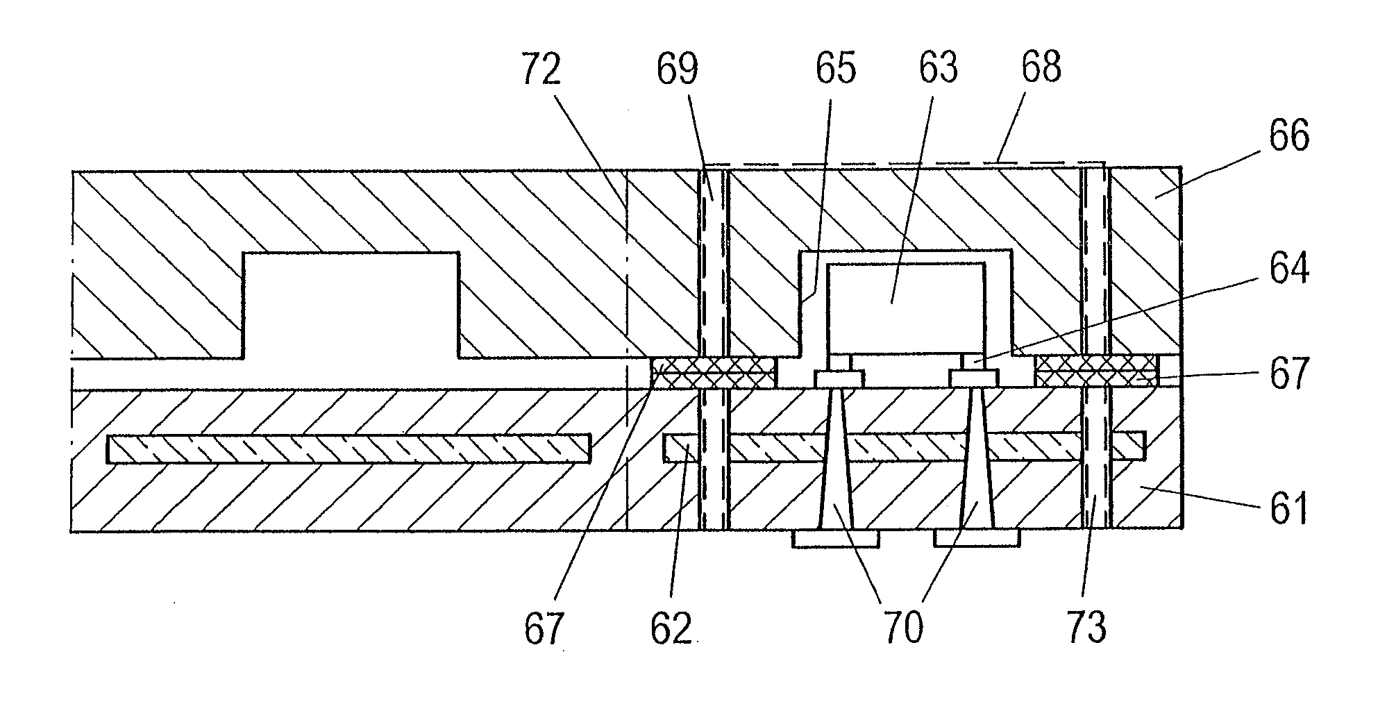
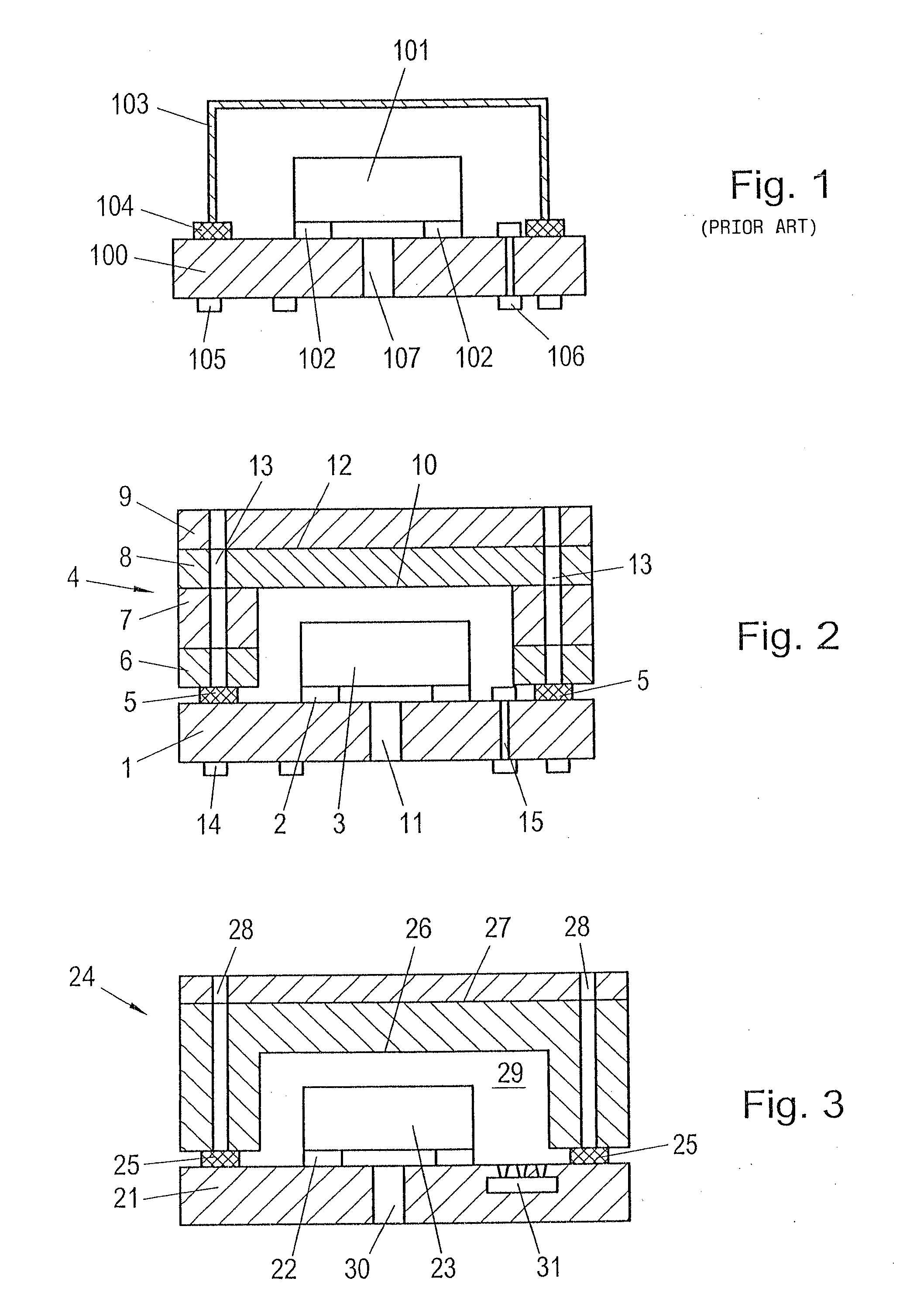
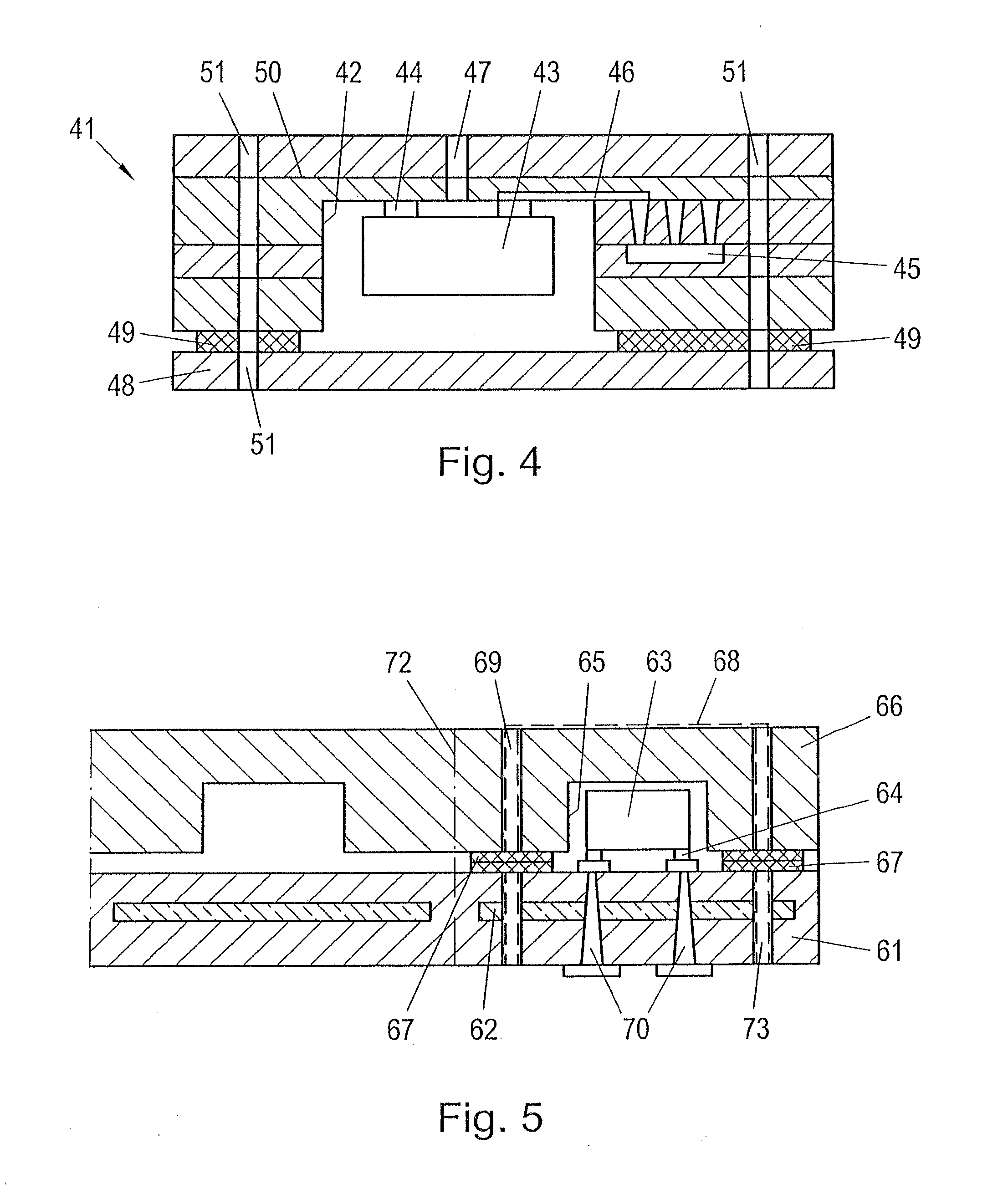
[0046]From the configuration according to the prior art as is schematically indicated in FIG. 1, it is apparent that an electronic component 101 is arranged on a printed circuit board element 100, which may, for instance, consist of a plurality of different layers or plies, which are not shown in detail, wherein only two contacts 102 are schematically indicated. The electronic component 101 is, for instance, formed by a microphone, wherein a metallic cage 103 is indicated to achieve appropriate shielding of the electronic component arranged on the printed circuit board element 100, said cage being connected, via connections 104, to conducting elements not illustrated in detail. Further contact connections of the printed circuit board, or structured conducting elements of the same, are schematically indicated by 105 and 106.

[0047]According to the prior art, an electronic component 101 to be additionally protected or shielded is thus arranged on a surface of a printed circuit board, w...


PUM

PropertyMeasurementUnit
Fractionaaaaaaaaaa
Fractionaaaaaaaaaa
Temperatureaaaaaaaaaa

Abstract

In a method for integrating a component (3) into a printed circuit board, the following steps are provided:
    • providing two completed printed circuit board elements (1, 4), which more particularly consist of a plurality of interconnected plies or layers (6, 7, 8), wherein at least one printed circuit board element (4) has a cutout or depression (10),
    • arranging the component (3) to be integrated on one of the printed circuit board elements (1) or in the cutout of the at least one printed circuit board element, and
    • connecting the printed circuit board elements (1, 4) with the component (3) being accommodated in the cutout (10), as a result of which it is possible to obtain secure and reliable accommodation of a component or sensor (3) in a printed circuit board.
Furthermore, a printed circuit board of this type comprising an electronic component (3) integrated therein is provided.

Description

[0001]This is a national stage of PCT / AT2011 / 000172 filed Apr. 11, 2011 and published in German, which has a priority of Austria, no. GM 236 / 2010 filed Apr. 13, 2010, hereby incorporated by reference.FIELD OF THE INVENTION [0002]The present invention relates to a method for integrating an electronic component into a printed circuit board, and a printed circuit board of this type, comprising an electronic component integrated therein.PRIOR ART [0003]In the context of the production of printed circuit boards having at least one electronic component integrated therein, it is known to accommodate such an electronic component in an, in particular multilayer, circuit board, particularly by adapting such multilayer circuit board layers or plies surrounding the component, whereupon methods known per se for connecting such, in particular different, layers of a multilayer circuit board are employed. In order to connect such layers or plies of a multilayer circuit board, such composite assembl...

Claims


Application Information

Patent Timeline
IPC IPC(8): H05K1/11H05K3/36H05K3/32
CPCH05K1/186H05K3/4623H05K3/4697H05K2201/0723H05K2201/09036Y10T29/49126H05K2201/09618H05K2201/10083H05K2201/10151Y10T29/49144H05K2201/09072H05K1/0218H05K1/0298H05K1/115H05K1/14H05K1/144H05K1/181H05K1/185H05K2201/041H05K2201/042H05K2201/043H05K2201/045H05K2201/10
Inventor STAHR, JOHANNESLEITGEB, MARKUS
Owner AT & S AUSTRIA TECH & SYSTTECHN AG
Why Eureka
Try Eureka