Systems and methods for row-wire voltage-loss compensation in crossbar arrays

a crossbar array and voltage loss compensation technology, applied in the field of micro- and nano-scale electronic devices, can solve the problems of many new obstacles, the fundamental component size limit will be reached in semiconductor-circuit-fabrication technology, and the need for far more technically demanding photolithographic methods

Active Publication Date: 2013-01-10
HEWLETT-PACKARD ENTERPRISE DEV LP
View PDF1 Cites 27 Cited by
  • Summary
  • Abstract
  • Description
  • Claims
  • Application Information

AI Technical Summary

Problems solved by technology

Eventually, however, it is expected that fundamental component-size limits will be reached in semiconductor-circuit-fabrication technologies based on photolithographic methods.
As the size of components decreases below the resolution limit of ultraviolet light, for example, far more technically demanding photolithographic methods may need to be employed.
Many new obstacles may be encountered.
As the component sizes decrease, precise alignment becomes more and more difficult and expensive.
As another example, the probabilities that certain types of randomly distributed defects in semiconductor surfaces result in defective semiconductor devices may increase as the sizes of components manufactured on the semiconductor surfaces decrease, resulting in an increasing proportion of defective devices during manufacture, and a correspondingly lower yield of useful product.
Ultimately, various quantum effects that arise only at molecular-scale distances may altogether overwhelm current approaches to semiconductor fabrication.
Although general wire technologies have been developed, it is not necessarily straightforward to employ nanowire technologies to miniaturize existing types of circuits and structures.
While it may be possible to tediously construct miniaturized, nanowire circuits similar to the much larger, currently available circuits, it is impractical, and often impossible, to manufacture such miniaturized circuits using current technologies.

Method used


Image

  • Systems and methods for row-wire voltage-loss compensation in crossbar arrays
  • Systems and methods for row-wire voltage-loss compensation in crossbar arrays
  • Systems and methods for row-wire voltage-loss compensation in crossbar arrays

Examples


Embodiment Construction

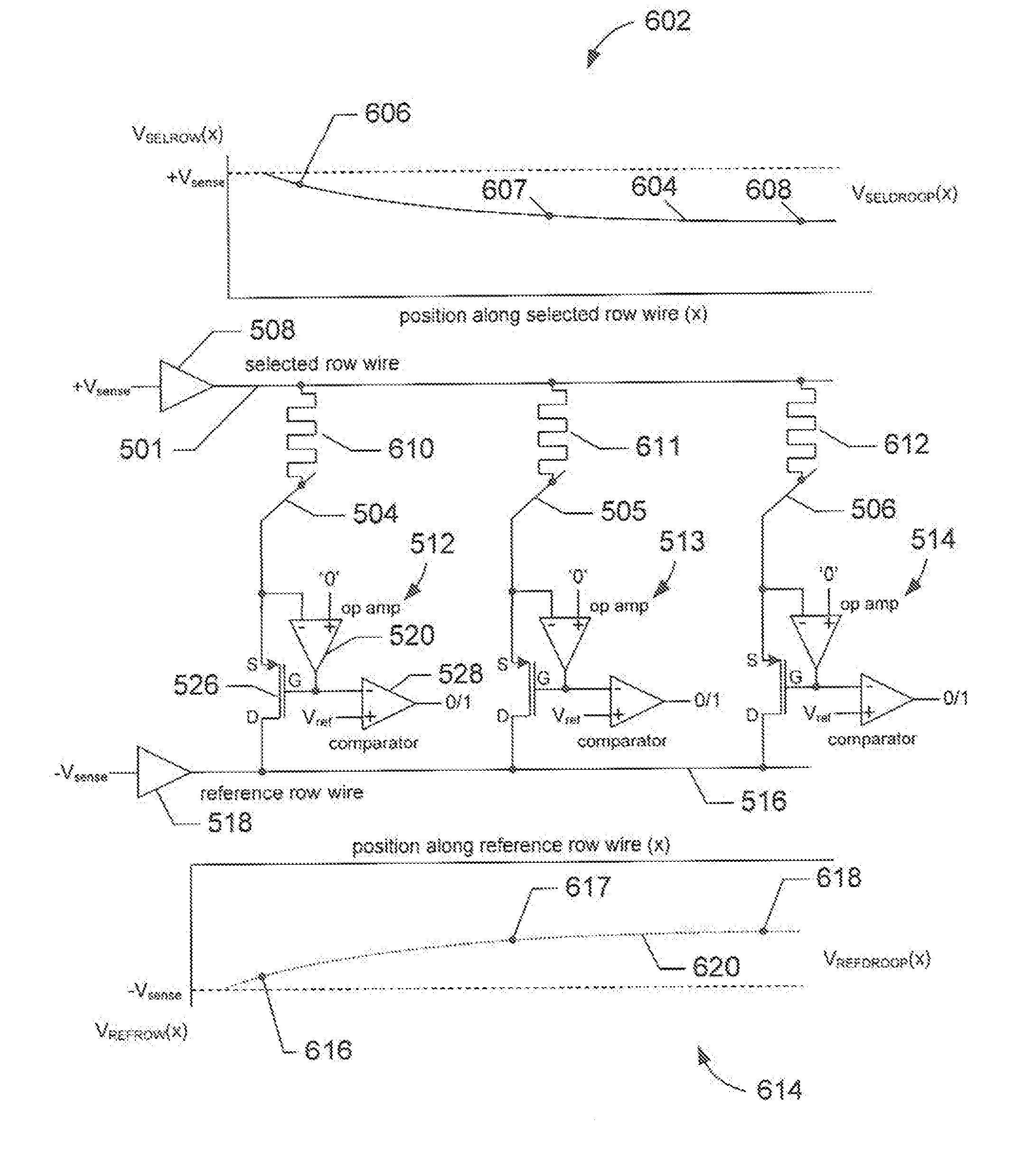
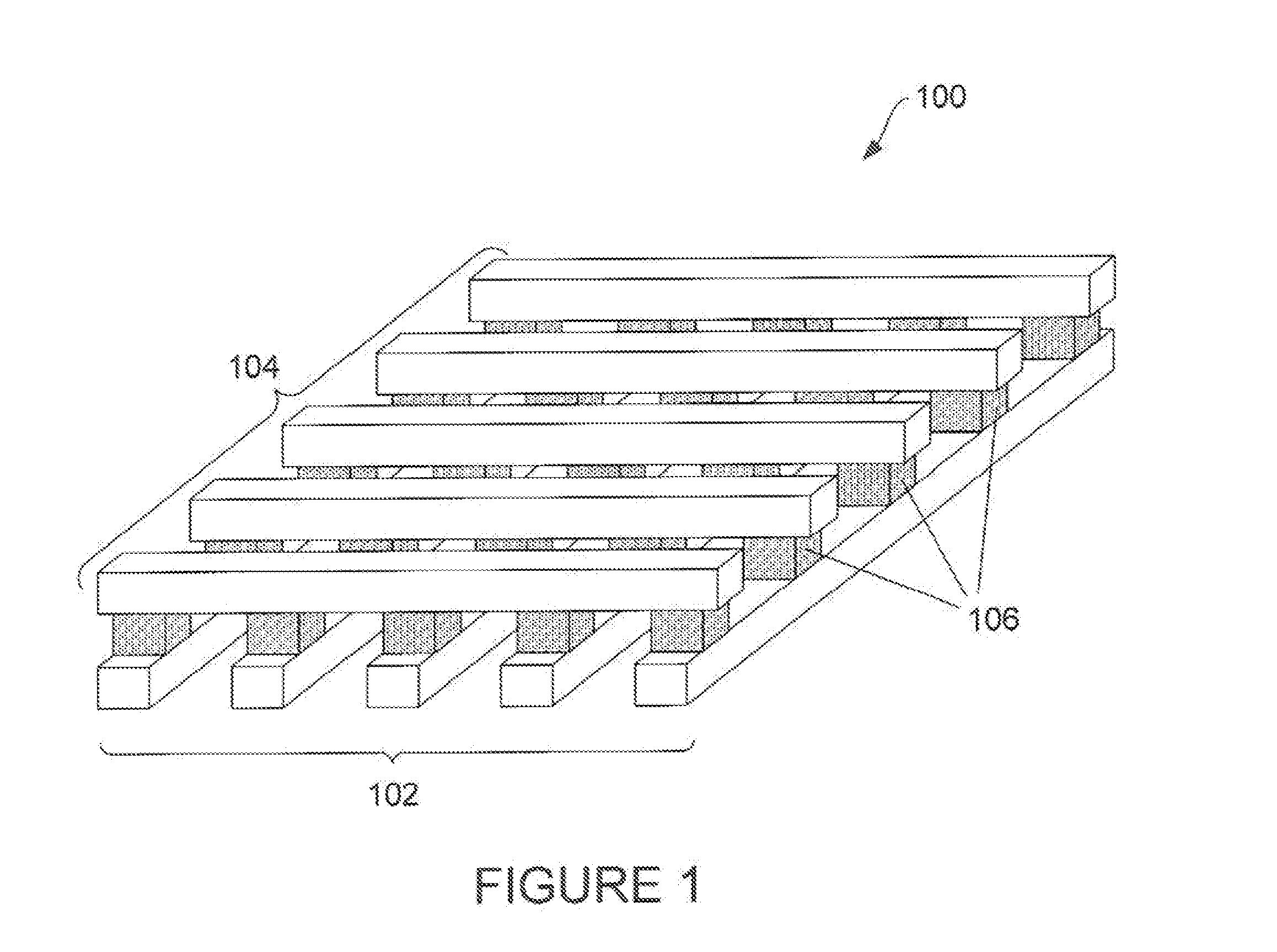
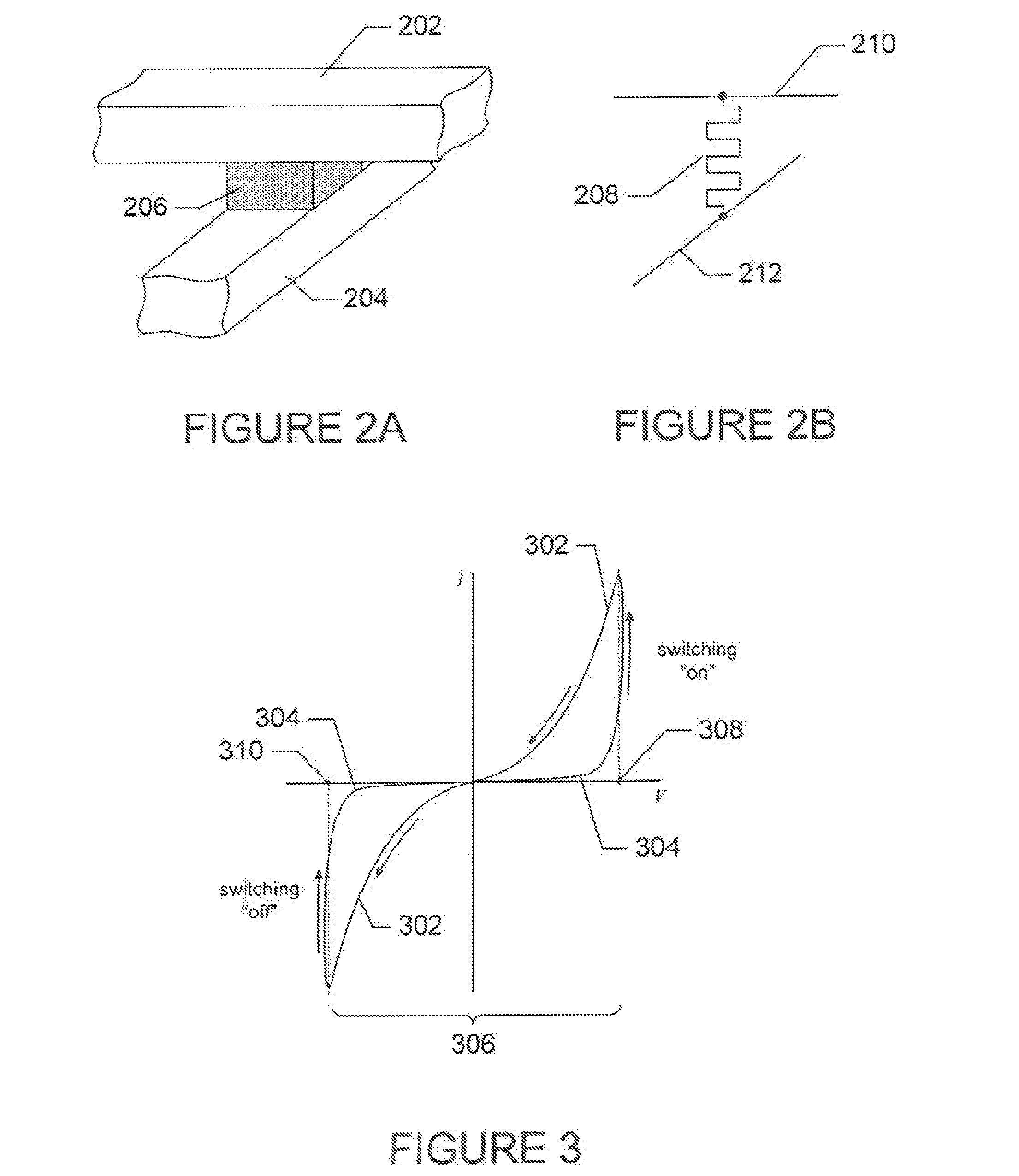
[0016]Embodiments of the present invention are directed systems and methods for reading the resistance states of crossbar junctions of a crossbar array. FIG. 1 shows an isometric view of a crossbar array 100 configured in accordance with one or more embodiments of the present invention. The crossbar array 100 is composed of a first layer of approximately parallel wires 102 called “column wires” that are overlain by a second layer of approximately parallel wires 104 called “row wises.” The row wires are approximately perpendicular, in orientation, to the column wires, although the orientation angle between the layers may vary. The two layers of wires form a lattice, or crossbar, each wire of the second layer 104 overlying all of the wires of the first layer 102 and coming into close contact with each wire of the first layer 102 at wire intersections that represent the closest contact between two overlapping wires. Wire intersections connected by devices 106 are called “crossbar junct...


PUM


Abstract

Embodiments of the present invention are directed systems and methods for reading the resistance states of crossbar junctions of a crossbar array. In one aspect, a system includes one or more sense amplifiers (512-514) connected to column wires of the crossbar array, a reference row wire (516) connected to each sense amp, and a wire driver (518) connected to the reference row wire and configured to drive the reference row wire. The sense amplifiers are configured so that when a selected row wire of the crossbar array is driven by a sense voltage, the column wires are held at approximately zero volts and pass currents through the column wires and sense amplifiers to the reference row wire so that resistive voltage losses along the reference row wire substantially mirror the resistive voltage losses along the selected row wire, allowing the sense amplifiers to determine the crossbar junction resistance states.

Description

STATEMENT OF GOVERNMENT INTEREST[0001]This invention has been made with Government support under Contract No. HR001 1-09-3-000, awarded by the Defense Advanced Research Projects Agency. The government has certain rights in the invention.TECHNICAL FIELD[0002]Embodiments of the present invention relate to microscale and nanoscale electronic devices, and in particular, to crossbar arrays.BACKGROUND[0003]During the past fifty years, the electronics and computing industries have been relentlessly propelled forward by ever decreasing sizes of basic electronic components, such as transistors and signal wires, and by correspondingly ever increasing component densities of integrated circuits, including processors and electronic memory chips. Eventually, however, it is expected that fundamental component-size limits will be reached in semiconductor-circuit-fabrication technologies based on photolithographic methods. As the size of components decreases below the resolution limit of ultraviolet...

Claims


Application Information

Patent Timeline
Patent Type & Authority Applications(United States)
IPC IPC(8): G11C11/21B82Y10/00
CPCG11C13/0002G11C13/0007G11C2213/77G11C13/0061G11C2013/0054G11C13/004
Inventor CARTER, RICHARD
Owner HEWLETT-PACKARD ENTERPRISE DEV LP
Why Eureka
Try Eureka