Cleaning method of semiconductor manufacturing process

Active Publication Date: 2013-01-17
UNITED MICROELECTRONICS CORP
View PDF5 Cites 2 Cited by
  • Summary
  • Abstract
  • Description
  • Claims
  • Application Information

AI Technical Summary

Benefits of technology

The present invention provides a cleaning method for a semiconductor manufacturing process that prevents the deposition of byproducts during cleaning, resulting in a smoother semiconductor component. The method also prevents uneven surfaces at the bottom of contact through holes, improving the component performance. The cleaning method includes a physical cleaning process and a chemical cleaning process, which removes oxide from the bottom of the contact through hole without increasing resistance or enlarging the size of the hole. The side wall of the semiconductor is smooth after the chemical cleaning process, and the byproduct can be removed through a thermal process, avoiding the deposition of byparticles during cleaning.

Problems solved by technology

However, currently, the components of the semiconductor integrated circuit become smaller and smaller.
Further, if a surface of a silicon layer is located at the bottom of the through hole, the physical bombardment process will cause the surface of the silicon layer to be uneven, thereby generating a leakage current problem and increasing a resistance of the corresponding component.

Method used


Image

  • Cleaning method of semiconductor manufacturing process
  • Cleaning method of semiconductor manufacturing process
  • Cleaning method of semiconductor manufacturing process

Examples


Embodiment Construction

[0035]The present invention will now be described more specifically with reference to the following embodiments. It is to be noted that the following descriptions of preferred embodiments of this invention are presented herein for purpose of illustration and description only. It is not intended to be exhaustive or to be limited to the precise form disclosed.

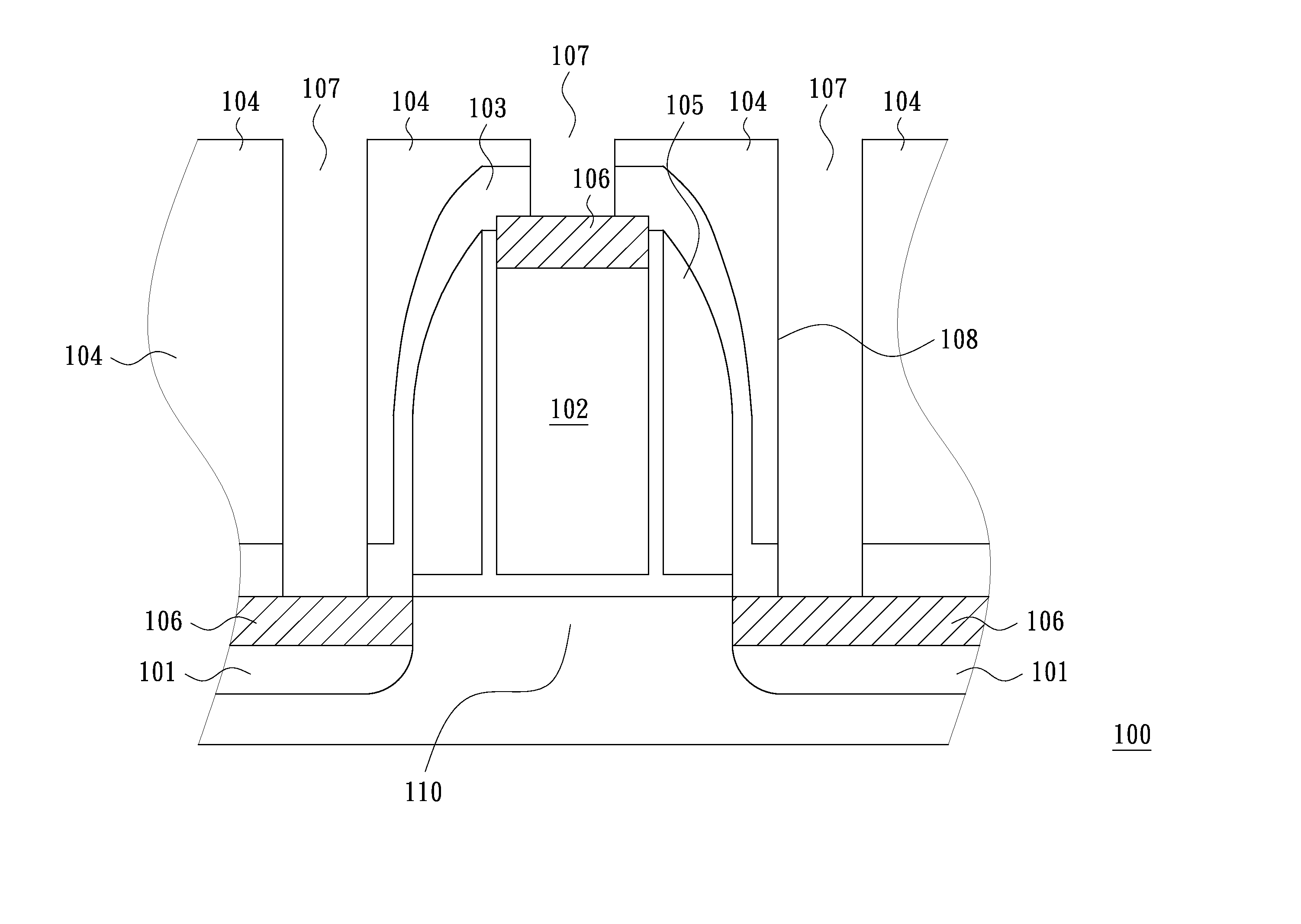
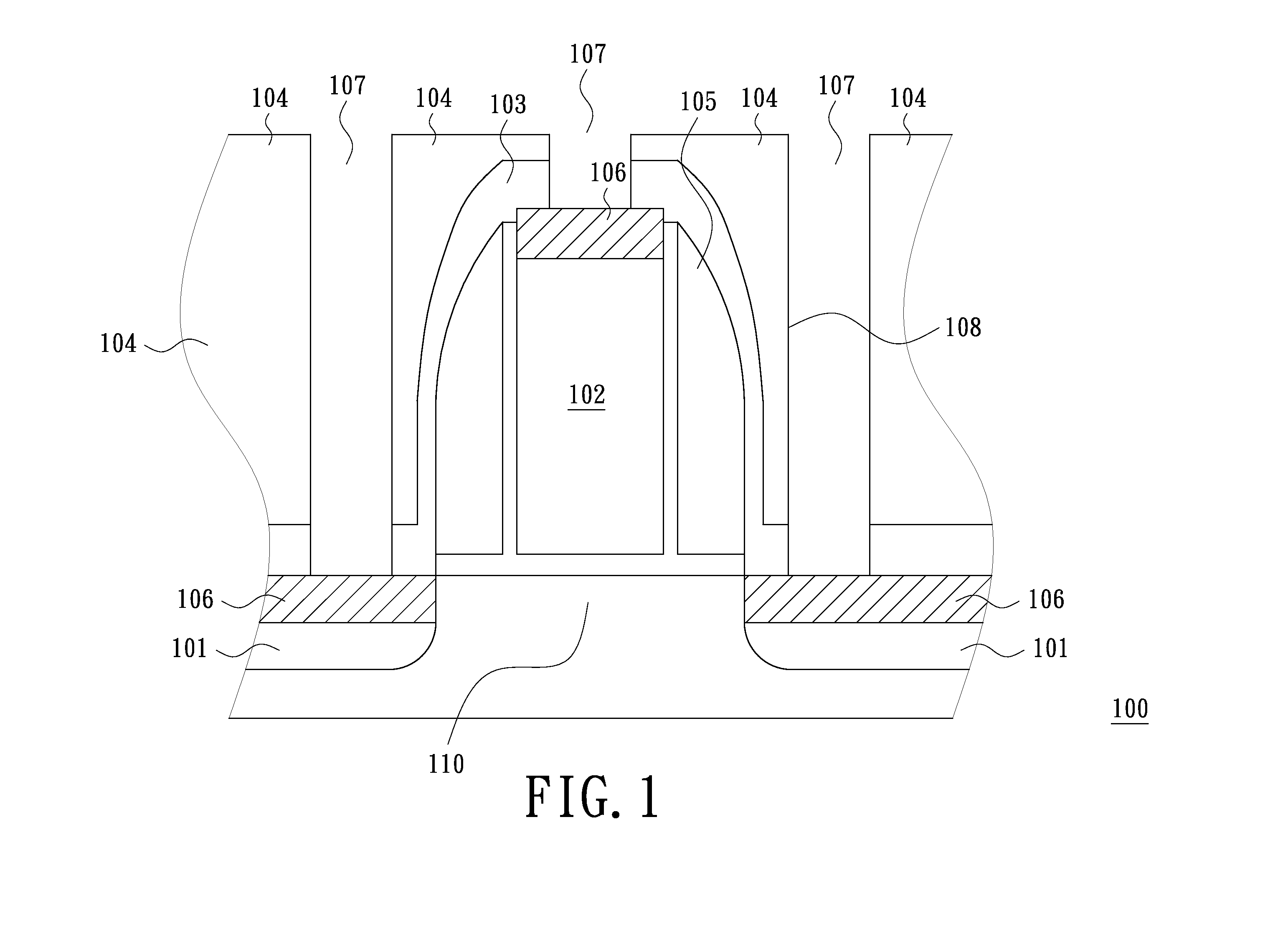
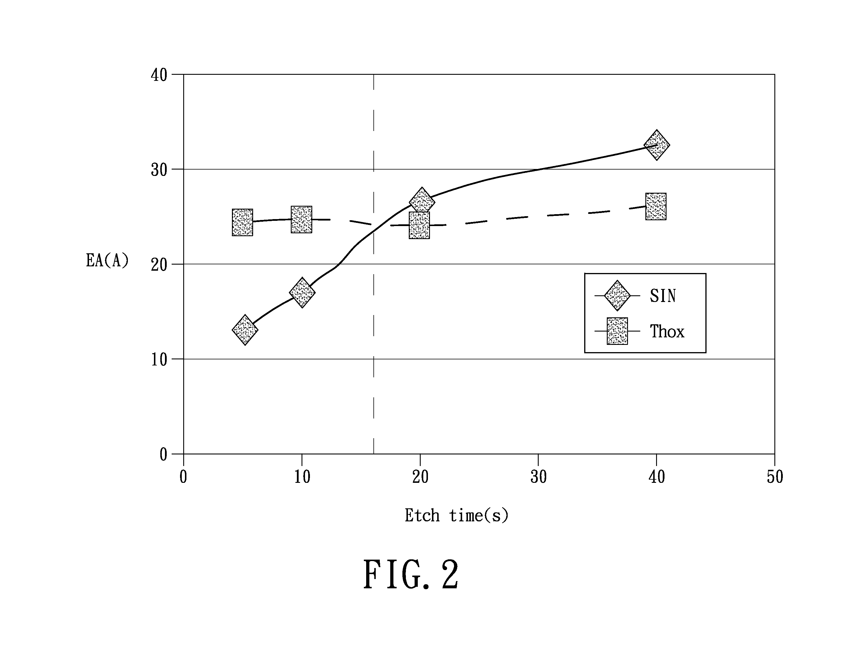
[0036]In order to solve the deposition phenomenon of the byproduct during the cleaning process and avoid the increase of the resistance of the component, a fluorine-based chemical cleaning process is developed so as to displace the physical bombardment process. However, the isotropic etching of the fluorine-based chemical cleaning process will enlarge the size of the contact through hole formed in the semiconductor component. The present invention provides a cleaning method of a semiconductor manufacturing process to reduce the resistance of the contact through hole of the semiconductor component and avoid enlarging the size of t...


PUM

PropertyMeasurementUnit
Temperatureaaaaaaaaaa
Timeaaaaaaaaaa

Abstract

A cleaning method of a semiconductor manufacturing process is provided. The cleaning method is applied to a semiconductor component including a plurality of material layers formed thereon. An opening is defined in the material layers, and a side wall is exposed from the opening The side wall at least includes a first material layer and a second material layer. At first, a first cleaning process is performed till a lateral etched thickness of the first material layer is equal to a lateral etched thickness of the second material layer. Then, a byproduct formed in the first cleaning process is removed.

Description

FIELD OF THE INVENTION[0001]The present invention relates to a cleaning method, and particularly to a cleaning method of a semiconductor manufacturing process.BACKGROUND OF THE INVENTION[0002]In a process of forming a semiconductor integrated circuit (IC), it is necessary to perform a cleaning process to clean various components of the semiconductor integrated circuit. A dry cleaning process, for example, a physical bombardment process, is generally used. The physical bombardment process utilities a number of free argon ions (Ar+) generated by argon (Ar) to remove oxides formed on surfaces of the components of the semiconductor integrated circuit. However, currently, the components of the semiconductor integrated circuit become smaller and smaller. For example, when a through hole formed in a component has a small size, a byproduct formed in the physical bombardment process will be deposited in the through hole. Thus, the size of the through hole will further be reduced. Further, if...

Claims


Application Information

Patent Timeline
IPC IPC(8): B08B7/04B08B5/00B08B3/08
CPCH01L21/76814H01L21/02063
Inventor CHEN, YI-WEITSAI, TENG-CHUNLAI, KUO-CHIHHUANG, SHU-MIN
Owner UNITED MICROELECTRONICS CORP
Why Eureka
Try Eureka