Semiconductor device and method of manufacturing semiconductor device

Active Publication Date: 2013-05-16
SEMICON ENERGY LAB CO LTD
View PDF2 Cites 6 Cited by
  • Summary
  • Abstract
  • Description
  • Claims
  • Application Information

AI Technical Summary

Benefits of technology

This patent describes a way to improve the performance of transistors that use an oxide semiconductor film. By reducing the contact resistance between the oxide semiconductor film and the metal film, the transistor's on-state characteristics can be improved. This results in a more efficient and reliable transistor that can be used in various applications.

Problems solved by technology

As described above, in the transistor that uses the oxide semiconductor film, the contact resistance between the metal film and the oxide semiconductor film degrades on-state characteristics of the transistor; thus, sufficient performance of a semiconductor device including the transistor might not be obtained.

Method used


Image

  • Semiconductor device and method of manufacturing semiconductor device
  • Semiconductor device and method of manufacturing semiconductor device
  • Semiconductor device and method of manufacturing semiconductor device

Examples


embodiment 1

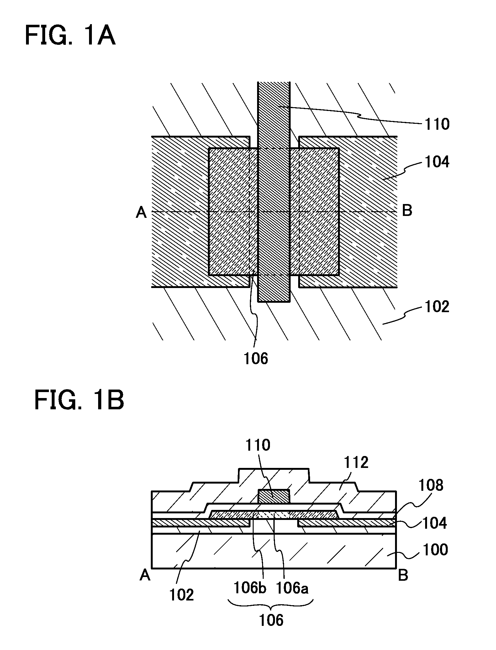
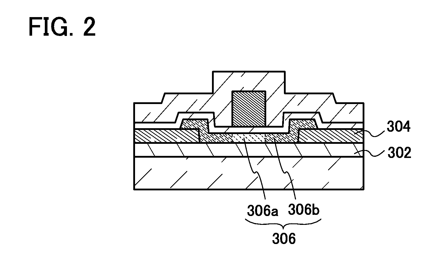
[0042]In this embodiment, transistors each of which is a semiconductor device of one embodiment of the present invention and a method of manufacturing the transistor will be described with reference to FIGS. 1A and 1B, FIG. 2, FIGS. 3A to 3C, and FIGS. 4A to 4C.

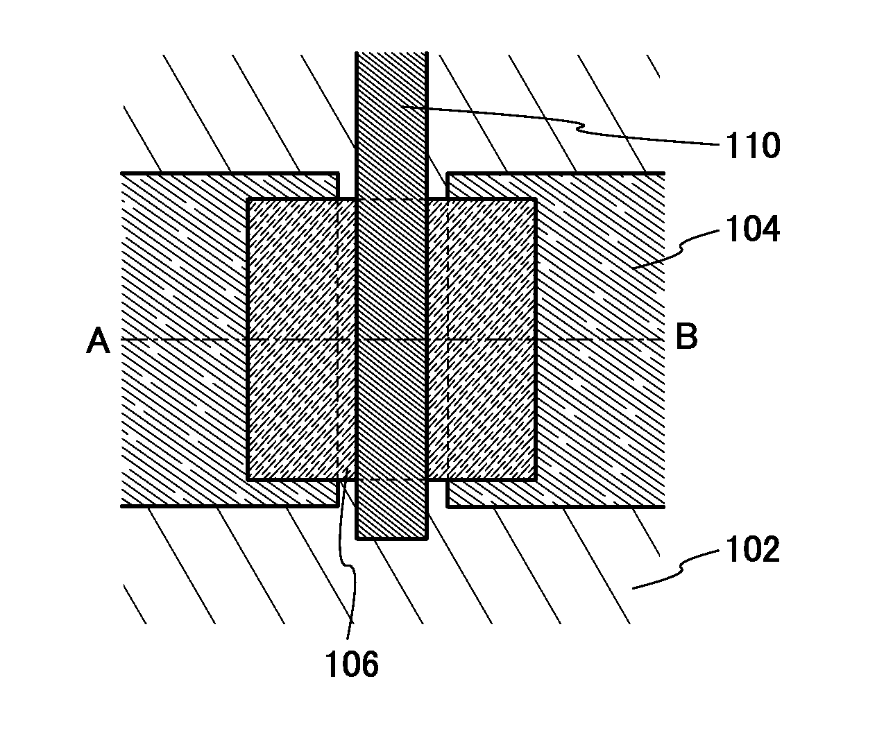
[0043]FIG. 1A is a top view and FIG. 1B is a cross-sectional view of a transistor which is a semiconductor device of one embodiment of the present invention. FIG. 1B illustrates a cross section A-B taken along a dashed-dotted line A-B in the top view of the transistor in FIG. 1A. Note that an interlayer insulating film 112, a gate insulating film 108, and the like are not illustrated in FIG. 1A for simplicity.

[0044]The transistor illustrated in FIG. 1B includes a base insulating film 102 over a substrate 100, a pair of electrodes 104 over the base insulating film 102, an oxide semiconductor film 106 in contact with the pair of electrodes 104, a gate insulating film 108 over the oxide semiconductor film 106, a gate electrode 1...

embodiment 2

[0107]In this embodiment, a transistor having a structure different from the structures of the transistors in Embodiment 1 and a method of manufacturing the transistor will be described with reference to FIGS. 5A and 5B and FIGS. 6A to 6C.

[0108]FIG. 5A is a top view and FIG. 5B is a cross-sectional view of a transistor which is a semiconductor device of one embodiment of the present invention. FIG. 5B illustrates a cross section A-B taken along a dashed-dotted line A-B in the top view of the transistor in FIG. 5A. Note that an interlayer insulating film 212, a gate insulating film 208, and the like are not illustrated in FIG. 5A for simplicity.

[0109]The transistor illustrated in FIG. 5B includes a base insulating film 202 over the substrate 100, a gate electrode 210 over the base insulating film 202, a gate insulating film 208 over the gate electrode 210, a pair of electrodes 204 over the gate insulating film 208, an oxide semiconductor film 206 overlapping with the gate electrode 2...

embodiment 3

[0126]In this embodiment, an example of manufacturing a semiconductor memory device using any of the transistors described in Embodiments 1 and 2 will be described.

[0127]Typical examples of a volatile semiconductor memory device include a dynamic random access memory (DRAM) which stores data in such a manner that a transistor included in a memory element is selected and electric charge is accumulated in a capacitor, and a static random access memory (SRAM) which holds stored data using a circuit such as a flip-flop.

[0128]Typical examples of a nonvolatile semiconductor memory device include a flash memory which has a node between a gate and a channel region of a transistor and stores data by holding electric charge in the node.

[0129]Any of the transistors described in Embodiments 1 and 2 can be applied to part of transistors included in the above-described semiconductor memory device.

[0130]First, a semiconductor memory device to which any of the transistors described in Embodiments 1...


PUM


Abstract

By reducing the contact resistance between an oxide semiconductor film and a metal film, a transistor that uses an oxide semiconductor film and has excellent on-state characteristics is provided. A semiconductor device includes a pair of electrodes over an insulating surface; an oxide semiconductor film in contact with the pair of electrodes; a gate insulating film over the oxide semiconductor film; and a gate electrode overlapping with the oxide semiconductor film with the gate insulating film interposed therebetween. In the semiconductor device, the pair of electrodes contains a halogen element in a region in contact with the oxide semiconductor film. Further, plasma treatment in an atmosphere containing fluorine can be performed so that the pair of electrodes contains the halogen element in a region in contact with the oxide semiconductor film.

Description

BACKGROUND OF THE INVENTION[0001]1. Field of the Invention[0002]The present invention relates to a semiconductor device and a manufacturing method thereof.[0003]Note that in this specification, a semiconductor device refers to any device that can function by utilizing semiconductor characteristics, and an electro-optical device, a semiconductor circuit, and an electronic device are all semiconductor devices.[0004]2. Description of the Related Art[0005]As materials of semiconductor thin films applicable to the transistors, silicon-based semiconductor materials have been widely used, but oxide semiconductors have been attracting attention as alternative materials.[0006]In many cases, transistors that use amorphous silicon, which can be manufactured using the established manufacturing technique, are utilized in display devices; however, the transistors that use amorphous silicon have low field-effect mobility, having difficulty in achieving high definition, low power consumption, and t...

Claims


Application Information

Patent Timeline
IPC IPC(8): H01L29/786H01L21/42
CPCH01L29/66969H01L29/41733H01L29/45H01L29/7869H01L29/78618H01L29/78636H01L29/78603
Inventor NODA, KOSEIENDO, YUTA
Owner SEMICON ENERGY LAB CO LTD
Why Eureka
Try Eureka