Solar cell and method for manufacturing same

Active Publication Date: 2018-03-08
KANEKA CORP
View PDF3 Cites 1 Cited by
  • Summary
  • Abstract
  • Description
  • Claims
  • Application Information

AI Technical Summary

Benefits of technology

The patent text describes a method to protect a p-type semiconductor layer during etching of an insulating layer. A protecting layer and insulating layer are applied in this order to stop etching of the insulating layer and prevent damage to the p-type semiconductor layer. This method prevents an increase in contact resistance and maintains an open circuit voltage.

Problems solved by technology

In a double-sided electrode type solar cell, shielding (shadowing loss) of sunlight by a metal electrode on the light-receiving side is a factor of reducing conversion efficiency.

Method used


Image

  • Solar cell and method for manufacturing same
  • Solar cell and method for manufacturing same
  • Solar cell and method for manufacturing same

Examples


examples

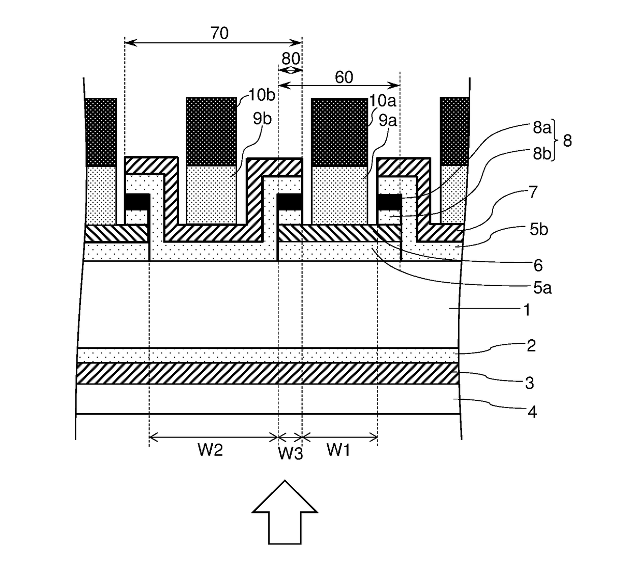
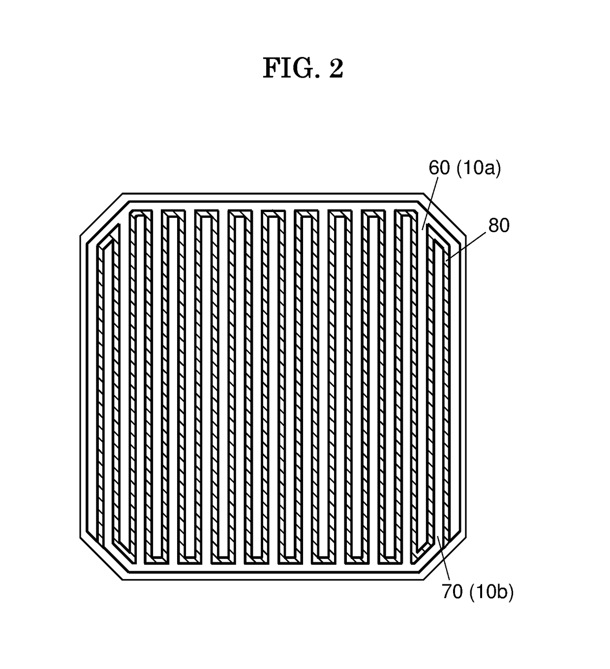
[0084]Hereinafter, the present invention will be described more in detail based on comparison between an example in which a crystalline silicon solar cell shown in FIG. 1 is prepared through steps shown in FIG. 3 and a comparative example in which a crystalline silicon-based solar cell is prepared through steps shown in FIG. 4. The present invention is not limited to the example described below.

example

[0085]A 200 μm-thick n-type single-crystalline silicon substrate having a (100) plane orientation on the incidence surface was immersed in a 2 wt % hydrofluoric acid aqueous solution for 3 minutes to remove a silicon oxide film on a surface of the substrate, and then rinsed with ultrapure water twice. The substrate was immersed for 15 minutes in a 5 / 15 wt % KOH / isopropyl alcohol aqueous solution held at 70° C., thereby obtaining a single-crystalline silicon substrate having pyramidal texture with (111) plane exposed on a surface thereof.

[0086]The texture-formed substrate was introduced into a CVD apparatus, and an i-type amorphous silicon layer was formed to have a thickness of 10 nm as an intrinsic silicon-based thin-film 2 on the light-receiving surface (second principal surface) side. Thereafter, an i-type amorphous silicon layer was formed to have a thickness of 8 nm as an intrinsic silicon-based thin-film 5a on the back surface (first principal surface) side. Deposition conditi...


PUM


Abstract

The solar cell includes an n-type semiconductor layer and a p-type semiconductor layer on a first principal surface of a crystalline silicon substrate. The n-type semiconductor layer is provided so as to extend over a part on a p-type semiconductor layer-formed region provided with the p-type semiconductor layer, and a p-type semiconductor layer non-formed-region where the p-type semiconductor layer is not provided. In a region where the n-type semiconductor layer is provided on the p-type semiconductor layer, a protecting layer is between the p-type semiconductor layer and the n-type semiconductor layer. The protecting layer includes: an underlying protecting layer that is in contact with the p-type semiconductor layer; and an insulating layer that is on the underlying protecting layer. The underlying protecting layer includes an intrinsic silicon-based layer or an n-type silicon-based layer.

Description

TECHNICAL FIELD[0001]The present invention relates to a solar cell and a method for manufacturing the same.BACKGROUND ART[0002]A general crystalline silicon-based solar cell is a double-sided electrode type solar cell, which includes a p-type semiconductor layer on one surface of a crystalline silicon substrate and an n-type semiconductor layer on the other surface of the crystalline silicon substrate, and either the p-layer-side or the n-layer-side is set to a light-receiving surface. On each of the light-receiving surface and the back surface, a metal electrode is provided for efficiently extracting a current. When sunlight is captured from the light-receiving surface, electron-hole pairs are generated in the crystalline silicon substrate, and a current is extracted through an electrode provided on each of the p-layer and the n-layer. In a double-sided electrode type solar cell, shielding (shadowing loss) of sunlight by a metal electrode on the light-receiving side is a factor of ...

Claims


Application Information

Patent Timeline
IPC IPC(8): H01L31/068H01L31/0747H01L31/18H01L31/20H01L31/0352H01L31/0216H01L31/0224
CPCH01L31/0682H01L31/0747H01L31/1896H01L31/20H01L31/0352H01L31/02167H01L31/022441H01L31/03529H01L31/1804H01L31/202Y02E10/547Y02P70/50
Inventor KAWASAKI, HAYATOYOSHIKAWA, KUNTANAKANO, KUNIHIROKONISHI, KATSUNORIYAMAMOTO, KENJI
Owner KANEKA CORP
Why Eureka
Try Eureka