Rapid fabrication methods for forming nitride based semiconductors based on freestanding nitride growth substrates

a technology of freestanding nitride and fabrication methods, which is applied in the direction of semiconductor lasers, lasers, solid-state devices, etc., can solve the problems of limiting the type of subsequent metal contacts that can be used, the cost and performance levels are insufficient for general lighting applications, and the effect of preventing solarization, yellowing and other degradation effects

Inactive Publication Date: 2013-01-24
GOLDENEYE
View PDF7 Cites 4 Cited by
  • Summary
  • Abstract
  • Description
  • Claims
  • Application Information

AI Technical Summary

Benefits of technology

[0008]This invention discloses the use of high temperature bonding and interconnect methods for devices based on freestanding nitride veneers. The use of inorganic glasses is a preferred embodiment of this invention. Even more preferred is the use of inorganic glasses which exhibit a CTE of between 20 and 100 / C. Most preferred is the use of inorganic glasses, which exhibit a CTE, which substantially matches the CTE of the freestanding nitride devices being packaged. The use of heating means includes, but is not limited to, laser welding, brazing, ovens, kilns, torches, furnaces, and IR lamps to melt the inorganic glasses such that bonding occurs between the inorganic glasses and the freestanding nitride devices. This bonding step can adhere an electrical interconnect means to at least one surface of the freestanding nitride devices. The electrical interconnect means may consist of, but is not limited to, a wire, foil, rod, or ball. Glass sealing metals, such as Kovar, dumet, and platinum, can ensure compatibility with the inorganic glass. The ability to melt bond contacts onto the freestanding nitride devices using inorganic glasses is disclosed. In this manner contacts and / or full / or partial encapsulation of the freestanding nitride devices can be realized very rapidly. Unlike organic solutions, inorganic glasses can provide hermetic sealing of the freestanding nitride devices or at least the contact regions of the freestanding nitride devices. For LED and other optoelectronic devices the use inorganic glasses is critical to preventing solarization, yellowing, and other degradation effects that plague existing high intensity LED applications. In order for high temperature processing to be possible the LED die themselves must be capable of being processed at these high temperatures.

Problems solved by technology

While this approach is useful in low intensity applications, the cost and performance levels are insufficient for general lighting applications.
This contact formation, however, forms a very thin diffusion based layer which is susceptible to aging and environmental effects.
The thinness of the diffusional layers also limits what type of subsequent metal contacts can be used.
Bow at room temperature adversely affects yield for contact formation and liftoff processes.
Bow at growth temperature leads to non-uniform device growth.
Excessive bow can also lead to wafer cracking which can lead to reactor damage.
The bimorph nature of a template also limits ramping times for any processes due to the potential of cracking of the whole wafer or the nitride film.
This leads to increased reactor process times and compromises on device structures.
These rapid temperature changes will crack even thin templates, especially for 3 and 4 inch wafers.
If the same thing is done to a template, the template will shatter violently.
Alternately, bulk nitride wafers are extremely expensive and must be surface polished which introduces surface defects.
Also because the bulk nitride wafers are sliced from a bowed thick growth, a variable miscut is created when a flat wafer is made.
Lastly, any useful device will require thinning to reduce the thermal impedance of the device.

Method used


Image

  • Rapid fabrication methods for forming nitride based semiconductors based on freestanding nitride growth substrates
  • Rapid fabrication methods for forming nitride based semiconductors based on freestanding nitride growth substrates
  • Rapid fabrication methods for forming nitride based semiconductors based on freestanding nitride growth substrates

Examples


Embodiment Construction

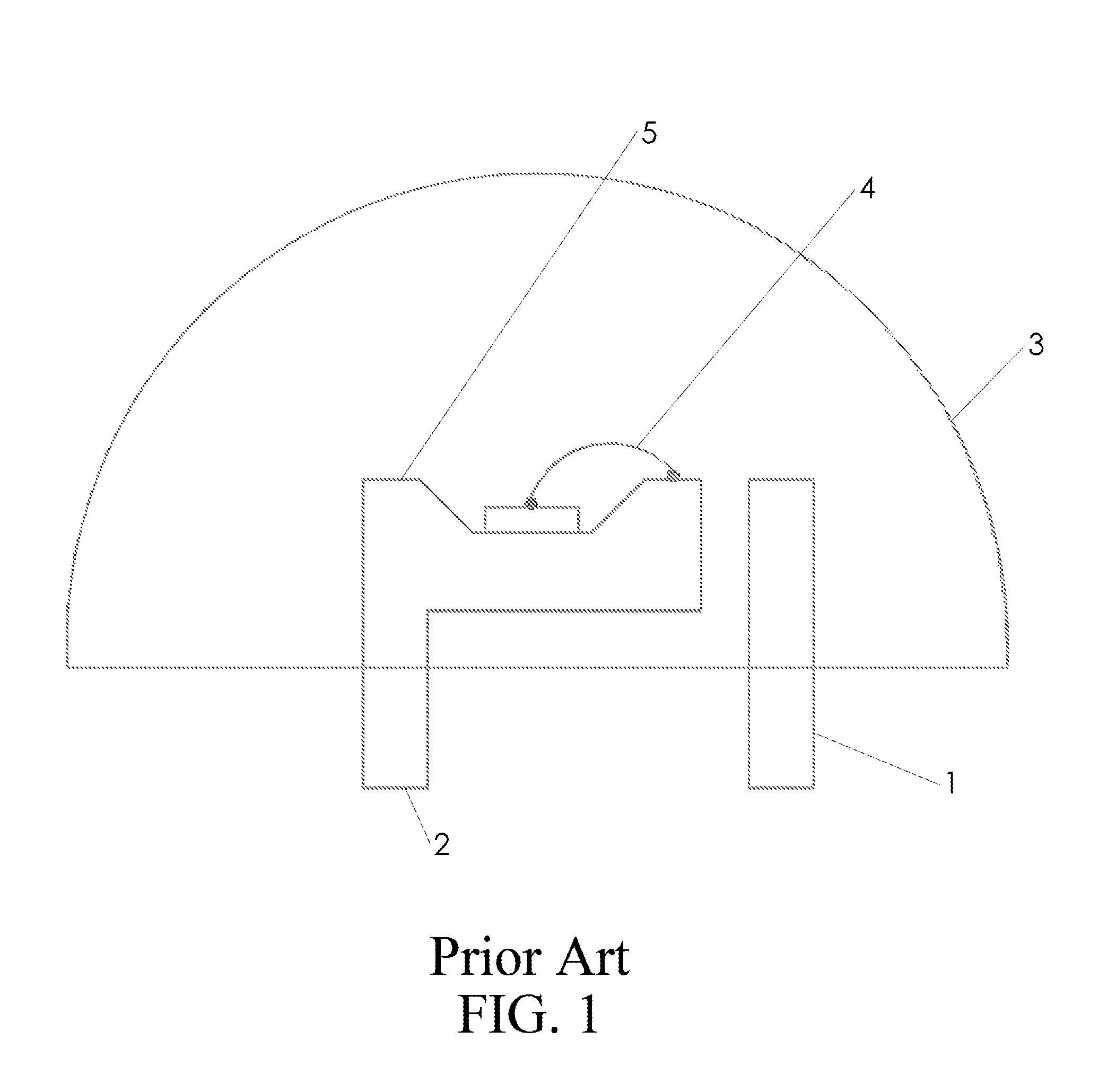
[0027]FIG. 1 depicts a standard LED. LED die 5 is typically mounted to contact pin 2 via a conductive epoxy. Wire bond 4 makes a connection between LED die 5 and contact pin 1. When a voltage is applied between contact pin 2 and contact pin 1, the LED die 5 emits light. Typically an organic encapsulant 3 surrounds the entire assembly to protect wire bond 4, environmentally protect the assembly, and improve light extraction and / or impart directionality to the emitted light from LED die 5. This approach is limited in its usage to low current applications due to the lack of thermal cooling and die size limitations. Organic encapsulants typically exhibit thermal conductivity less than 0.1 w / m / K.

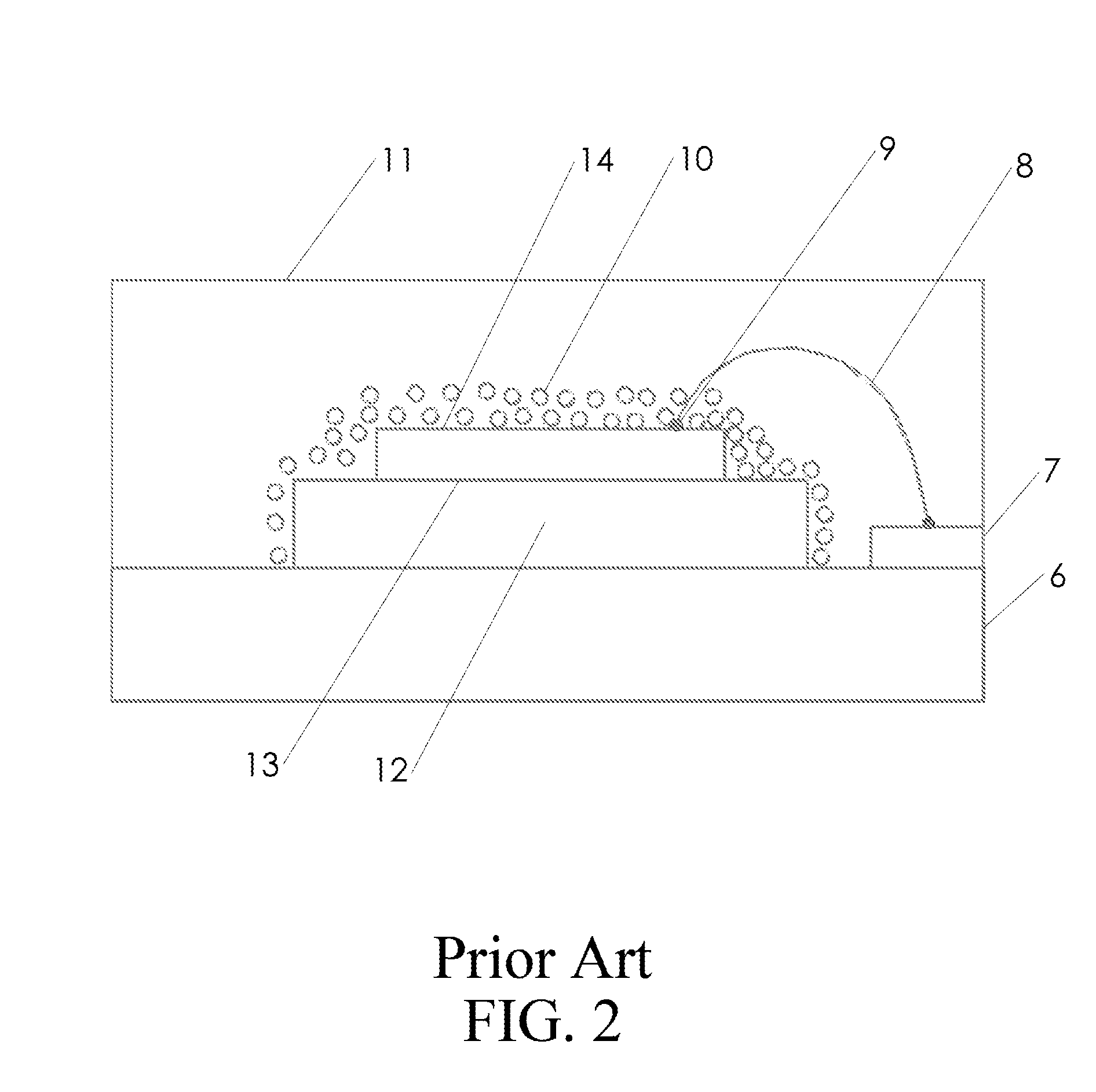
[0028]FIG. 2 depicts a typical white LED. Active region 14 is waferbonded via a solder 13 to LED substrate 12. Submount 6 provides thermal spreading and interconnect means for the assembly. Heat generation is localized in active region 14 and propagates through solder 13 through LED substrate 12 ...
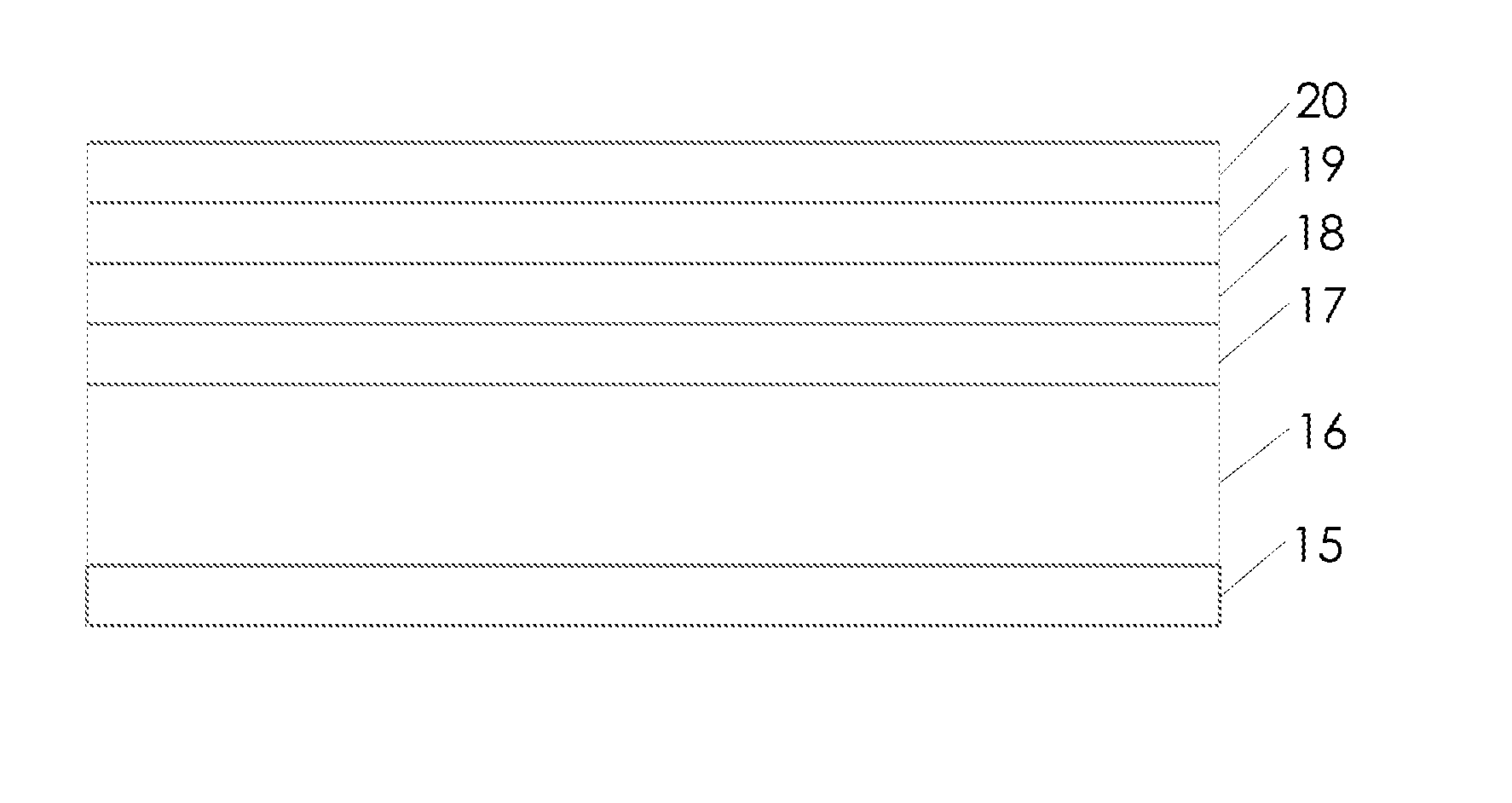

PUM

PropertyMeasurementUnit
thicknessaaaaaaaaaa
thickaaaaaaaaaa
thickaaaaaaaaaa

Abstract

High temperature bonding and interconnect methods can be used for LED and other optoelectronic devices based on freestanding nitride devices. Inorganic glasses, especially those which exhibit a CTE, which substantially matches the CTE of the freestanding nitride devices, can provide hermetic sealing of the freestanding nitride devices or the contact regions of the freestanding nitride devices. The freestanding nitride devices are typically freestanding nitride veneers.

Description

REFERENCE TO PRIOR APPLICATION[0001]This application claims the benefit of U.S. Provisional Patent Application Ser. No. 61 / 572,768, which was filed on Jul. 21, 2011, which is herein incorporated by reference.BACKGROUND OF THE INVENTION[0002]Light emitting diodes (LEDs) are typically fabricated using standard semiconductor packaging techniques. Die are mounted using epoxy or solder onto a submount, interconnect is via wirebonding or flip chip methods, and then organic encapsulants are formed over the assembly. While this approach is useful in low intensity applications, the cost and performance levels are insufficient for general lighting applications. Optoelectronics, electronics, solar, and sensors applications can also benefit from lower cost higher performance devices. The need therefore exists for novel fabrication methods, which reduce cost and enable electronic, optical, and optoelectronic applications.[0003]Presently rapid thermal annealing creates ohmic contacts in nitride b...

Claims


Application Information

Patent Timeline
Patent Type & Authority Applications(United States)
IPC IPC(8): H01L29/20
CPCH01L25/0753H01L25/0756H01L2924/13091B82Y20/00H01L2924/3011H01L2224/8592H01L2224/48247H01L27/153H01L33/0075H01L33/42H01L33/50H01S5/0206H01S5/02284H01S5/34333H01L2224/48091H01L2924/00H01L2224/73265H01L2924/181H01L2224/48257H01S5/02251H01L2924/00014H01L2924/00012H01L29/20
Inventor ZIMMERMAN, SCOTT M.LIVESAY, WILLIAM R.ROSS, RICHARD L.
Owner GOLDENEYE
Why Eureka
Try Eureka