Optical Proximity Correction Method

Active Publication Date: 2013-01-24
UNITED MICROELECTRONICS CORP
View PDF1 Cites 13 Cited by
  • Summary
  • Abstract
  • Description
  • Claims
  • Application Information

AI Technical Summary

Benefits of technology

[0010]The present invention provides an optical proximity correction method and a circuit pattern formed by the method. The bridge phenom

Problems solved by technology

When the light passes through the mask, diffraction occurs and reduces resolution.
Moreover, when light passes through the transparent regions of a mask having different interval sizes, the light through the regions having small

Method used


Image

  • Optical Proximity Correction Method
  • Optical Proximity Correction Method
  • Optical Proximity Correction Method

Examples


Embodiment Construction

[0015]To provide a better understanding of the presented invention, preferred embodiments will be made in detail. The preferred embodiments of the present invention are illustrated in the accompanying drawings with numbered elements.

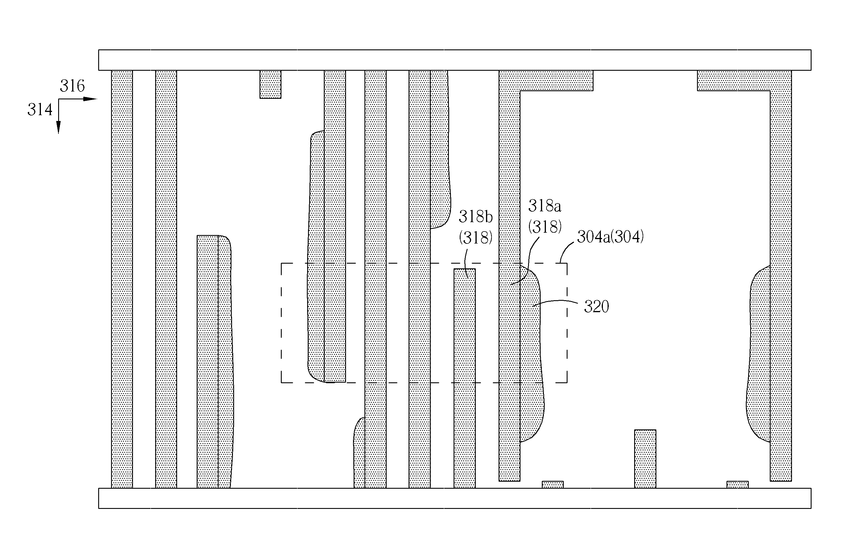
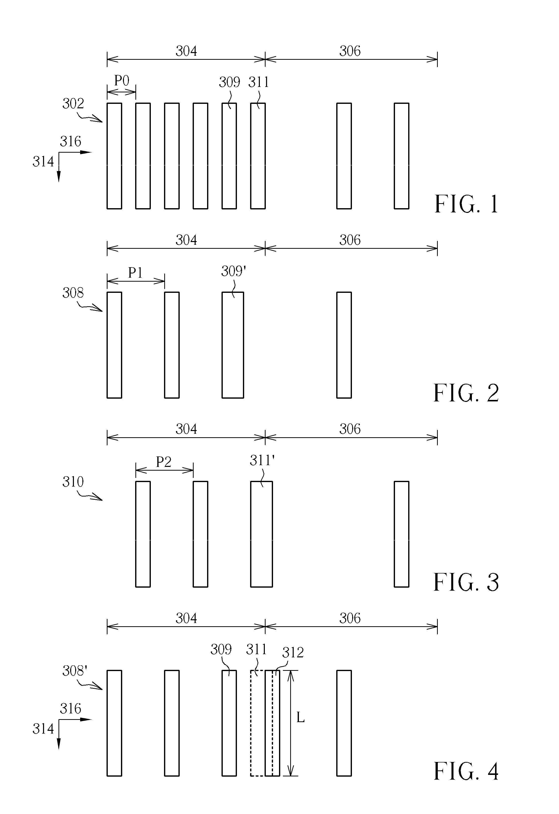
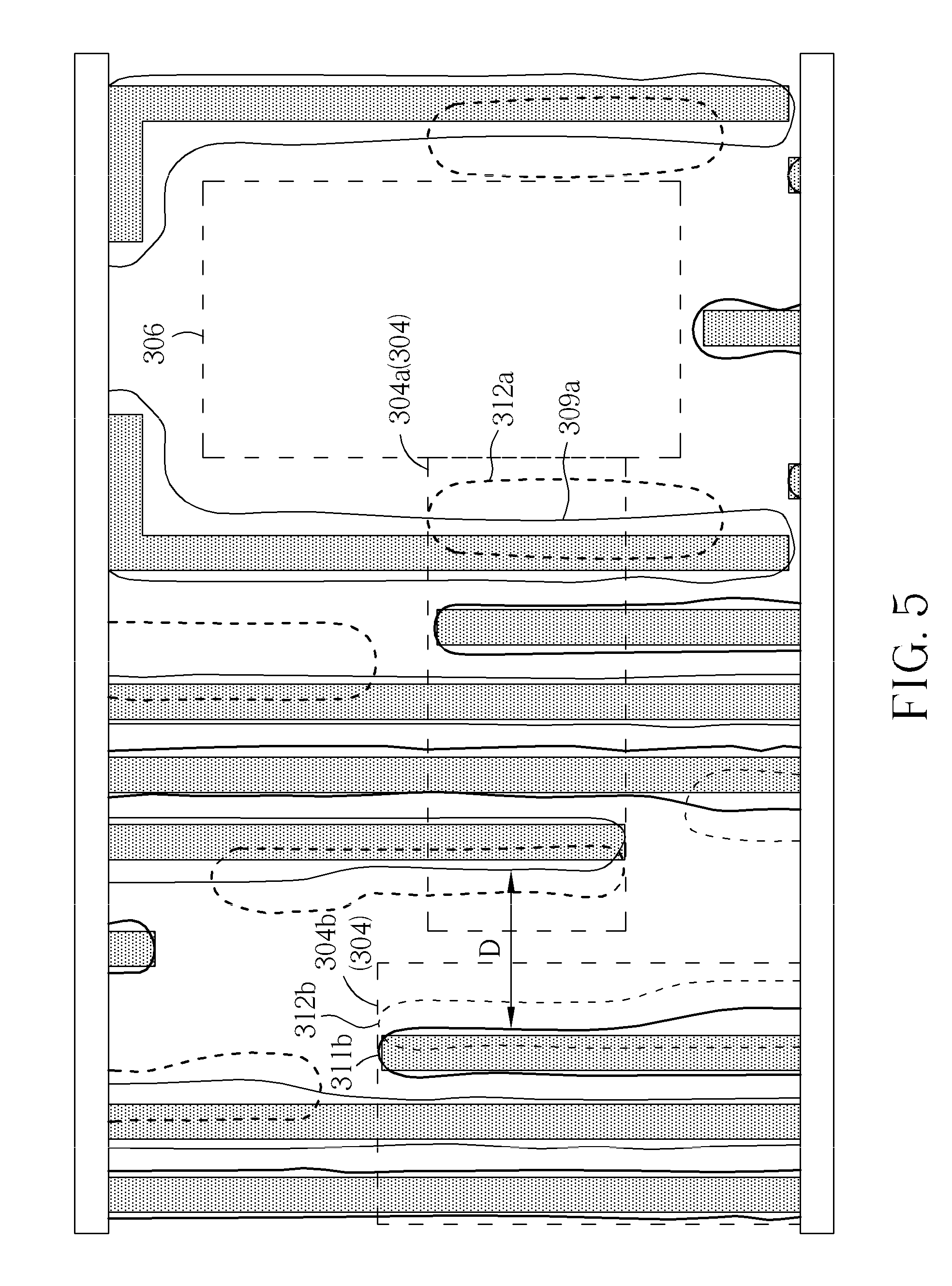
[0016]Please refer to FIG. 1 to FIG. 4, illustrating schematic diagrams of the optical proximity correction method in the present invention. As shown in FIG. 1, a target pattern 302 is provided. For example, the target pattern 302 is input into a computer system (not shown). The target patterns 302 refers to the final pattern which will be formed on the semiconductor photoresist layer (not shown) in the followed up steps and reflects the layout of the electrical circuit. According to the degree of density, the target pattern 302 can be divided into a dense region 304 which has a larger pattern density per unit area and an isolated region 306 which has a smaller pattern density per unit area. In the dense region 304, the target pattern 302 usually compris...


PUM


Abstract

An optical proximity correction method is provided. A target pattern is provided, and then the target pattern is decomposed to a first pattern and a second pattern. The first pattern and the second pattern are alternately arranged in a dense region. Then, a compensation pattern is provided and it is determined whether the compensation pattern is added into the first pattern to become a first revised pattern, or into the second pattern to become a second revised pattern. Finally, the first revised pattern is output onto a first mask and the second revised pattern is output onto a second mask.

Description

BACKGROUND OF THE INVENTION[0001]1. Field of the Invention[0002]The present invention relates to an optical proximity correction method, and more particularly, to an optical proximity correction method which uses a compensation pattern and can be applied to a double exposure technique.[0003]2. Description of the Prior Art[0004]In semiconductor manufacturing processes, in order to transfer an integrated circuit layout onto a semiconductor wafer, the integrated circuit layout is first designed and formed as a photo-mask pattern. The photo-mask pattern is then proportionally transferred to a photoresist layer positioned on the semiconductor wafer.[0005]In recent years, with the increasing miniaturization of semiconductor devices, the design rule of line width and space between lines or devices becomes finer. However, the width is subject to optical characteristics. To obtain fine-sized devices in the exposure, the interval between transparent regions in a mask is scaled down with devic...

Claims


Application Information

Patent Timeline
IPC IPC(8): G06F17/50
CPCG03F1/36G03F1/70G03F7/70466G03F7/70441
Inventor HUANG, CHIA-WEICHEN, MING-JUITSENG, TING-CHENGKUO, HUI-FANG
Owner UNITED MICROELECTRONICS CORP
Why Eureka
Try Eureka