Display device

a technology of a display device and a sealing member, which is applied in the direction of identification means, instruments, non-linear optics, etc., can solve the problems of liquid crystal material of the liquid crystal layer leaking, the likelihood of leakage the spread of liquid crystal material around the region, so as to achieve effective reduction or prevention of aligned film material, excellent endurance, and reduced distance between aligned film and sealing member

Active Publication Date: 2013-01-31
SHARP KK
View PDF8 Cites 51 Cited by
  • Summary
  • Abstract
  • Description
  • Claims
  • Application Information

AI Technical Summary

Benefits of technology

[0026]In the display device of the present invention, if the groove is formed in a continuous annular shape and is provided in the substrate outer perimeter portion to surround the display region, in the second substrate an annular rib protruding toward the first substrate and surrounding the display region is preferably formed in a region corresponding to the groove of the first substrate as viewed from above, and the rib preferably has a protrusion height from a substrate surface which is smaller than or equal to a depth of the groove, and a width of the rib which is smaller than a width of the groove corresponding to the rib.
[0016]Also, with the above configuration, the underlying metal is provided below the groove in at least regions which the groove overlaps the first group of interconnects as viewed from above. Therefore, even if the groove extends across the first group of interconnects, the first group of interconnects are not exposed from the groove surface, or conduction is not established between a conductive film provided on the groove surface and the first group of interconnects. Therefore, it is not likely that a short circuit is made between the first group of interconnects via the conductive film provided on the groove surface or conductive foreign matter existing in the vicinity of the groove surface, or that the first group of interconnects are exposed from the groove surface and are corroded. Also, even if the underlying metal makes contact with the conductive film provided on the groove surface or conductive foreign matter existing in the vicinity of the groove surface, or the first group of interconnects are exposed from the groove surface, the display performance of the display device is not affected, because the underlying metal is not an interconnect which is directly involved in driving of the display device. Therefore, excellent endurance can be obtained.

Problems solved by technology

Incidentally, when inkjet printing is used to form the alignment film, a resin material having a lower viscosity than that used in flexographic printing is used as a material for the alignment film, and therefore, the alignment film material is likely to leak and spread into a region around a region (display region) in which the alignment film should be printed.
Therefore, if the non-display region around the display region is so small that a large space cannot be ensured between the display region and the sealing member region, the alignment film may flow into the sealing member region.
In this case, the adhesiveness between the sealing member and the alignment film is insufficient, and therefore, the gap between the two substrates cannot be completely sealed, so that the liquid crystal material of the liquid crystal layer may leak.

Method used


Image

  • Display device
  • Display device
  • Display device

Examples


first embodiment

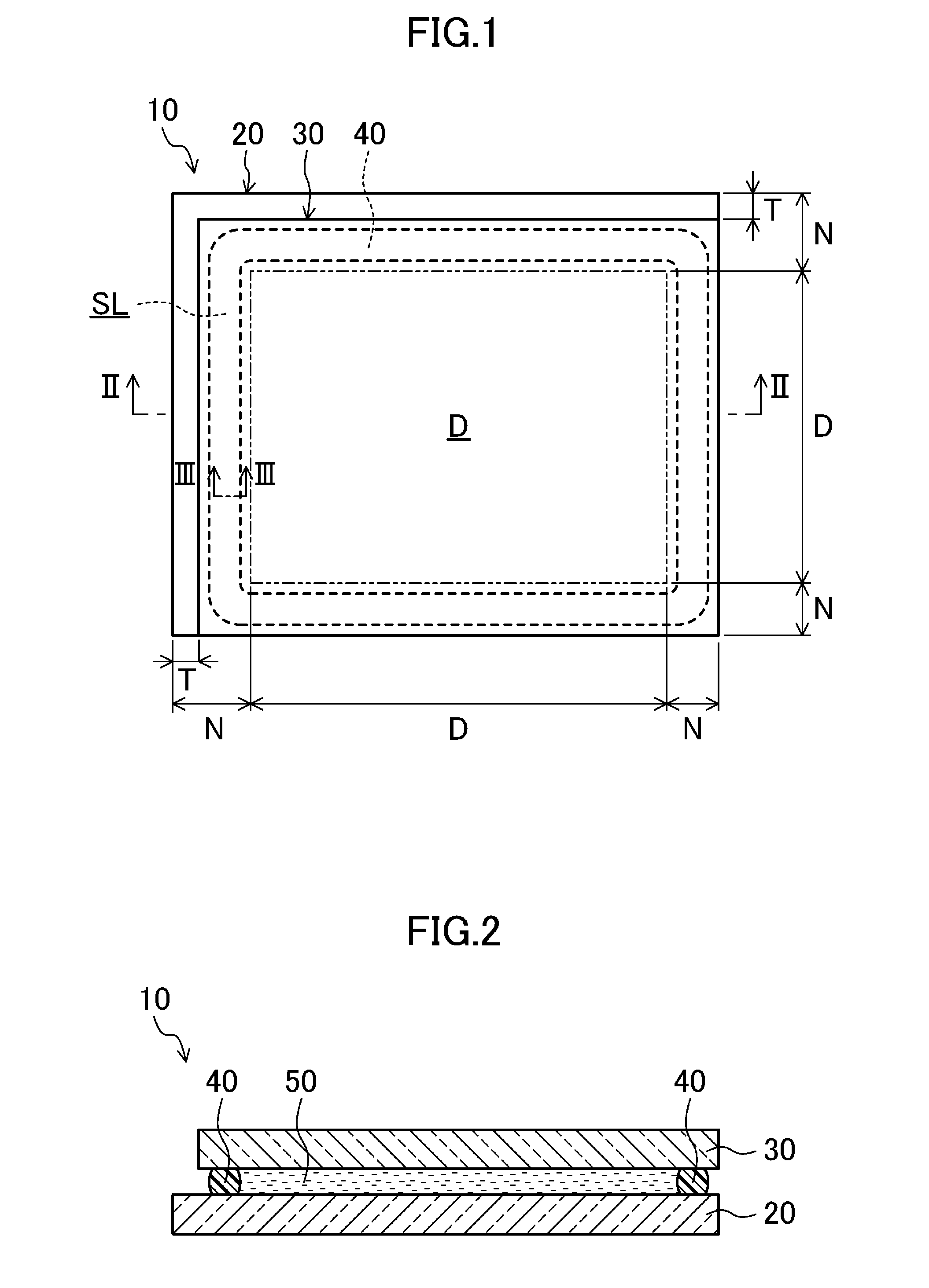
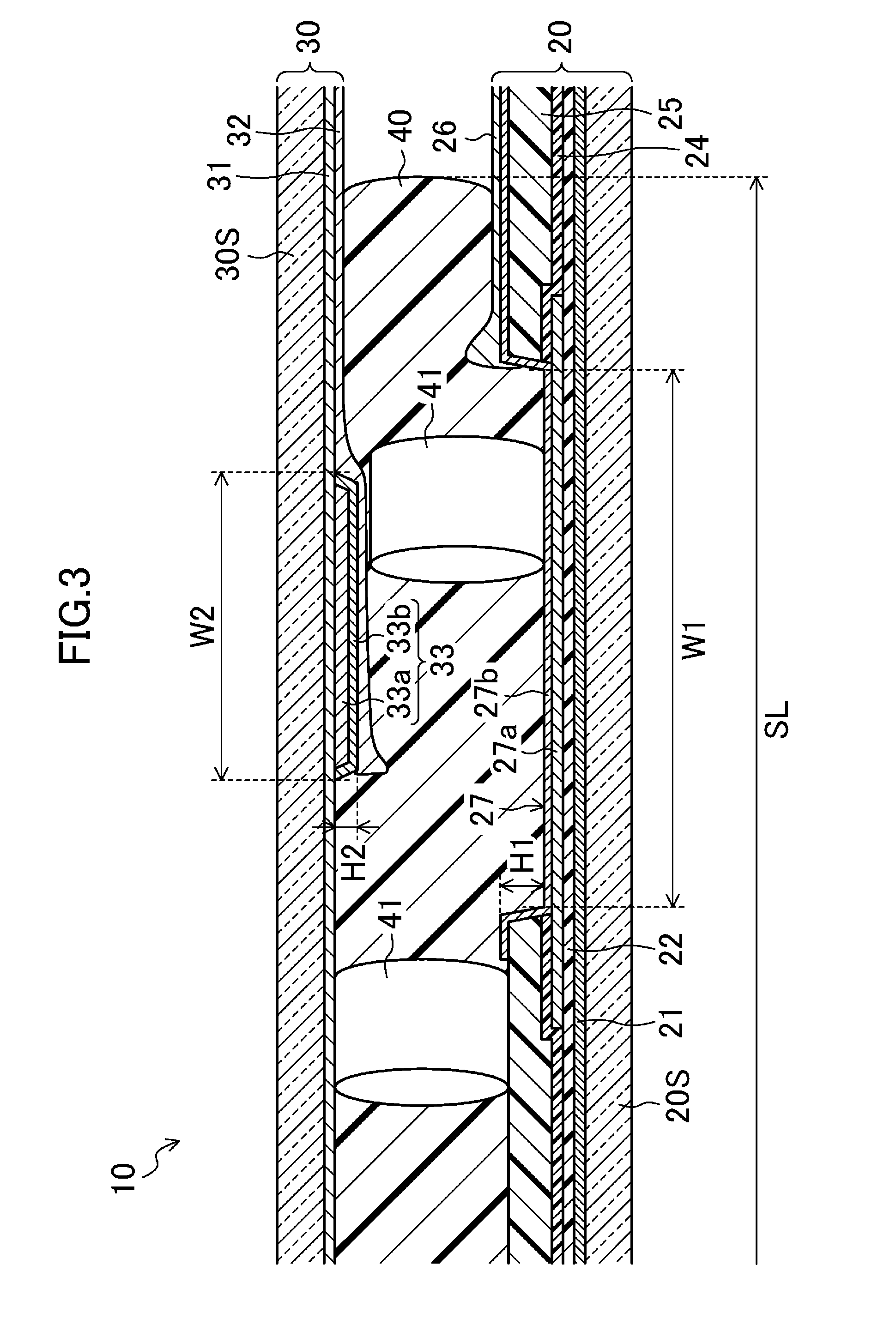
[0084]FIGS. 1 and 2 schematically show an entire liquid crystal display device 10 according to a first embodiment. FIG. 3 is an enlarged cross-sectional view of the liquid crystal display device 10 in the vicinity of a seal region SL thereof. FIGS. 4 and 5 are plan views of an array substrate 20 and a counter substrate 30, respectively.

[0085]The liquid crystal display device 10 includes the array substrate 20 (first substrate) and the counter substrate 30 (second substrate), which face each other. The array substrate 20 includes a first metal (first group of interconnects) including gate lines 21, a gate insulating film 22, a second metal (second group of interconnects) including source lines 23 (see FIG. 6), a passivation film 24, a planarization film 25, a third metal including pixel electrodes (not shown), and an alignment film 26, which are formed and stacked together on a substrate body 20S. A detailed configuration of the array substrate 20 will be described below. The counter...

second embodiment

[0128]Next, a liquid crystal display device 10 according to a second embodiment will be described. Note that parts which are the same as or corresponding to those of the first embodiment are indicated by the same reference characters as those of the first embodiment.

[0129]The liquid crystal display device 10 includes an array substrate 20 and a counter substrate 30 which face each other and are bonded together by a sealing member 40 provided in an outer perimeter portion thereof, and a liquid crystal layer 50 as a display layer in a space enclosed by the sealing member 40. The liquid crystal display device 10 has the same configuration as that of the first embodiment, except for the array substrate 20.

[0130]As in the first embodiment, the array substrate 20 includes a first metal including gate lines 21, a gate insulating film 22, a second metal including source lines 23, a passivation film 24, a planarization film 25, a third metal including pixel electrodes, and an alignment film ...

third embodiment

[0137]Next, a liquid crystal display device 10 according to a third embodiment will be described.

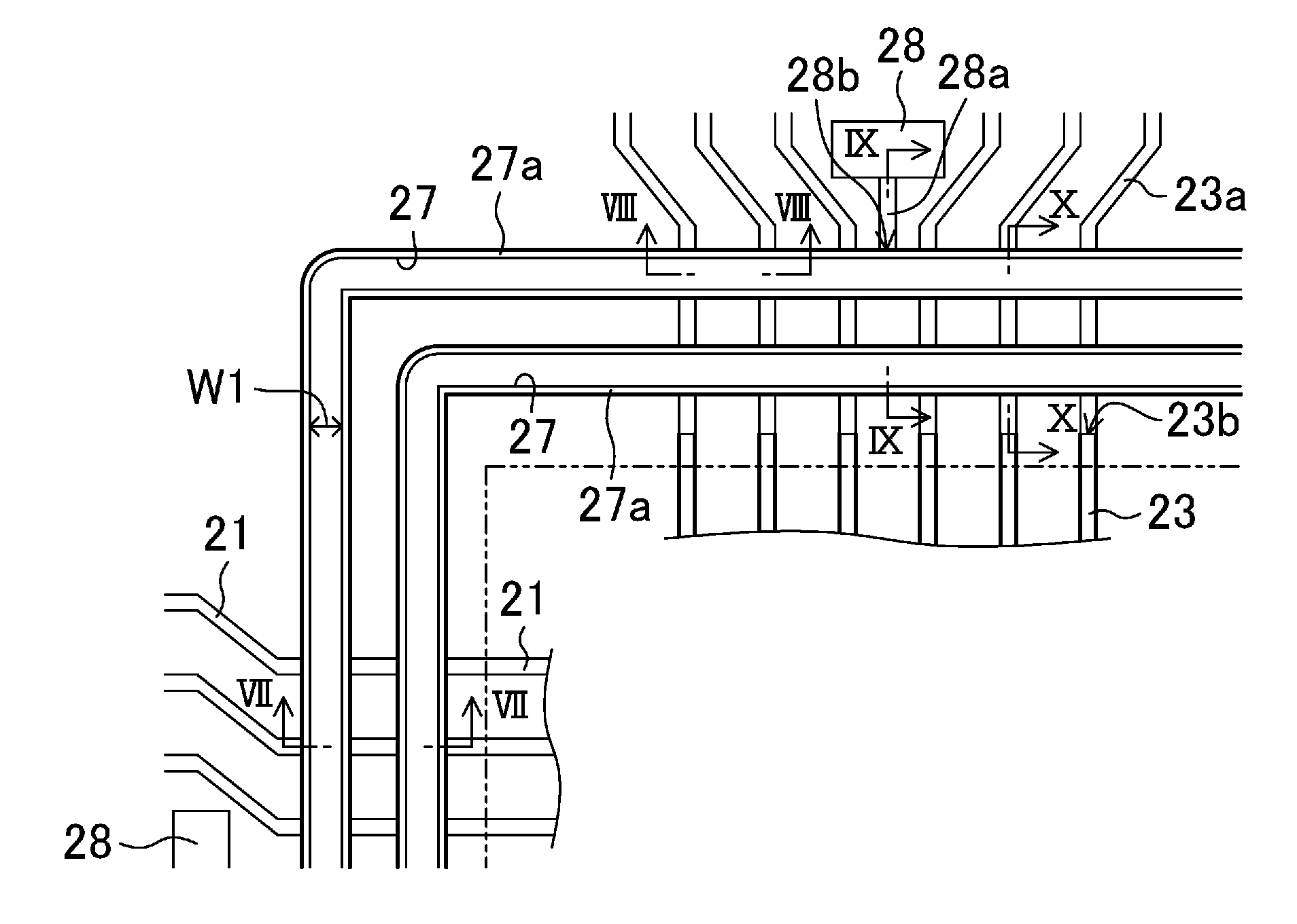
[0138]FIG. 27 is a diagram schematically showing the entire liquid crystal display device 10 of the third embodiment. The enlarged cross-sectional view of an area in the vicinity of a seal region SL of the liquid crystal display device 10 is similar to that of the first embodiment shown in FIG. 3. FIGS. 28 and 29 are plan views of an array substrate 20 and a counter substrate 30, respectively. Note that parts which are the same as or corresponding to those of the first embodiment are indicated by the same reference characters as those of the first embodiment.

[0139]The liquid crystal display device 10 includes the array substrate 20 and the counter substrate 30, which face each other and are bonded together by a sealing member 40 provided in an outer perimeter portion (seal region SL) thereof, and a liquid crystal layer 50 as a display layer in a space enclosed by the sealing member 40. A...


PUM

PropertyMeasurementUnit
widthaaaaaaaaaa
diameteraaaaaaaaaa
thicknessaaaaaaaaaa

Abstract

A groove (27) is formed above a first group of interconnects (21, 23a) of a first substrate, continuously extending along a substrate outer perimeter portion and across the first group of interconnects (21, 23a). An underlying metal (27a) is provided in the same layer in which a second group of interconnects (23) are provided, below the groove (27) in at least regions in which the groove (27) overlaps the first group of interconnects (21, 23a) as viewed from above.

Description

TECHNICAL FIELD[0001]The present invention relates to display devices, such as a liquid crystal display device, etc., and more particularly, to a structure around a groove provided in a picture-frame region for controlling a region in which an alignment film is applied.BACKGROUND ART[0002]Liquid crystal display devices can have a smaller thickness and lower power consumption, and therefore, are widely used as a display for a mobile information apparatus, such as a television set, an OA apparatus (e.g., a personal computer, etc.), a mobile telephone, a personal digital assistant (PDA), etc.[0003]A liquid crystal display device includes a liquid crystal display panel, and a backlight unit attached to the back surface of the liquid crystal display panel. The liquid crystal display panel includes an array substrate including switching elements (e.g., thin film transistors, etc.), and a counter substrate facing the array substrate, which are bonded together by a sealing member. A liquid ...

Claims


Application Information

Patent Timeline
Patent Type & Authority Applications(United States)
IPC IPC(8): G02F1/1333
CPCG02F1/136286G02F1/1345G02F1/1333G09F9/30
Inventor MORIWAKI, HIROYUKI
Owner SHARP KK
Why Eureka
Try Eureka