Phase change structure with composite doping for phase change memory

a phase change memory and composite doping technology, applied in the field of memory devices, can solve problems such as data errors, memory cells made of phase change materials can fail, and dimension phase change devices involve endurance, and achieve the effect of improving enduran

Inactive Publication Date: 2011-03-03
MACRONIX INT CO LTD +1
View PDF99 Cites 47 Cited by
  • Summary
  • Abstract
  • Description
  • Claims
  • Application Information

AI Technical Summary

Benefits of technology

[0016]A memory device is described herein with composite doping. The device includes a first electrode, a phase change material, such as a chalcogenide, in contact with the first electrode, and a second electrode in contact with the phase change material. The phase change material comprises a first dopant characterized by tending to segregate on grain boundaries in the active region, and a second dopant characterized by bonding with an element or elements of the phase change material in the active region to improve endurance, such as by causing an increase in recrystallization temperature of, and / or suppressing void formation in, the phase change material in the active region.
[0017]The first dopant comprises a stable, segregating material such as a dielectric, which can be selected for a chalcogenide based memory material, from silicon oxide, aluminum oxide, silicon carbide and silicon nitride. The second dopant comprises a material that forms relatively strong bonds with an element of the phase change material, increasing the melting temperature and the recrystallization temperature, which can improve endurance and retention, and suppressing void formation under the thermal stress in the active region, which can prevent device failure cause by such voids.
[0018]The stoichiometry of a phase change material tends to change inside the active region of the device, relative to that outside the active region because of the more extreme thermal conditions there, as the materials tend to migrate to more stable combinations according to the thermal environment. By doping the phase change material with a reactive dopant that tends to strengthen the phase change material, such as by forming a compound having a higher melting point or having a higher recrystallization temperature at which amorphous phase to crystalline phase transition occurs, in the active region, the endurance and retention of the memory device are dramatically improved.
[0019]For example, for a chalcogenide including Te and Sb, the second dopant is a reactive material like Si that bonds with the Te with a bonding energy greater than a bonding energy between the Te and the Sb. This may be a result of formation in the active region of a mixture of materials including higher melting point Si—Te compounds that tend to stabilize the microstructure in the active region, suppressing void formation, and resulting in higher endurance and better data retention.

Problems solved by technology

One problem with very small dimension phase change devices involves endurance.
Specifically, memory cells made using phase change materials can fail as the composition of part of the phase change material slowly changes with time from the amorphous to the crystalline phase.
If these crystalline regions connect to form a low resistance path through the active region, when the memory cell is read, a lower resistance state will be detected and result in a data error.
Another problem with phase change memory cells arises from the manufacturability issues arising from the polycrystalline phase of the material.
A large grain size can result in void formation that interferes with current flow in unexpected ways, and can cause failure.
However, it is found that gas phase dopants like nitrogen and oxygen, while causing a reduction in grain size in the deposited material, have not been reliable, and result in void formations in the material during use.
Although substantial benefits are achieved as taught in application Ser. No. 12 / 286,874 from relatively high concentration doping with silicon dioxide, as compared with nitrogen, including reduction in grain size in the polycrystalline phase and suppression of the formation of multiple crystalline phases, endurance issues still arise.

Method used


Image

  • Phase change structure with composite doping for phase change memory
  • Phase change structure with composite doping for phase change memory
  • Phase change structure with composite doping for phase change memory

Examples


Embodiment Construction

[0035]A detailed description of the present invention is provided with reference to FIGS. 1-11.

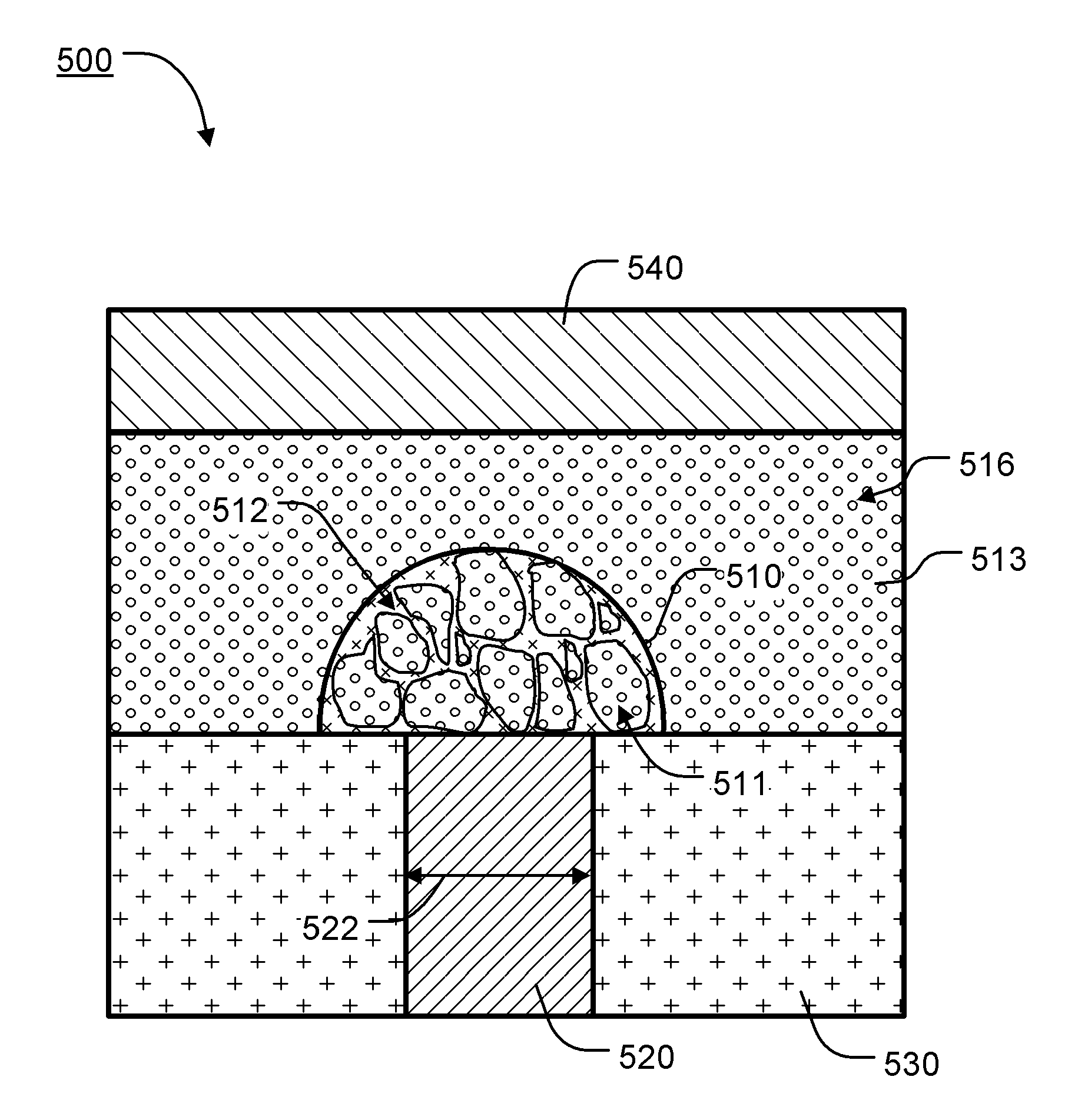
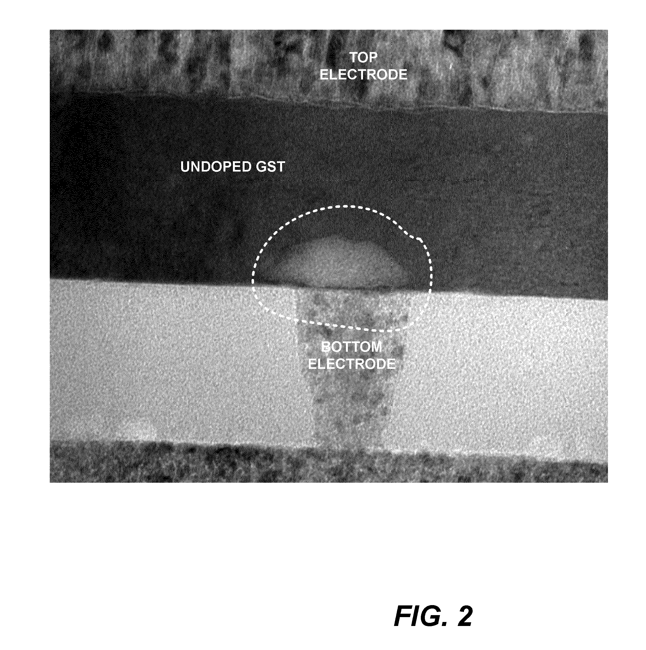
[0036]FIG. 1 illustrates a cross-sectional view of a memory cell 500 having a composite doped active region 510 comprising phase change domains 511 within a dielectric-rich mesh 512 caused by segregation of the first dopant on grain boundaries of the phase change material, and a more stable phase change material having a higher recrystallization temperature in the active region as a result of the second reactive dopant.

[0037]The memory cell 500 includes a first electrode 520 extending through dielectric 530 to contact a bottom surface of the memory element 516, and a second electrode 540 on the memory element 516 consisting of a doped phase change material. The first and second electrodes 520, 540 may comprise, for example, TiN or TaN. Alternatively, the first and second electrodes 520, 540 may each be W, WN, TiAlN or TaAlN, or comprise, for further examples, one or more elements selected ...


PUM


Abstract

A memory device is described using a composite doped phase change material between a first electrode and a second electrode. A memory element of phase change material, such as a chalcogenide, is between the first and second electrodes and has an active region. The phase change material has a first dopant, such as silicon oxide, characterized by tending to segregate from the phase change material on grain boundaries in the active region, and has a second dopant, such as silicon, characterized by causing an increase in recrystallization temperature of, and / or suppressing void formation in, the phase change material in the active region.

Description

PARTIES TO A JOINT RESEARCH AGREEMENT[0001]International Business Machines Corporation, a New York corporation, and Macronix International Corporation, Ltd., a Taiwan corporation, are parties to a Joint Research Agreement.BACKGROUND OF THE INVENTION[0002]1. Field of the Invention[0003]The present invention relates to memory devices based on phase change materials including chalcogenide materials, and methods for manufacturing such devices.[0004]2. Description of Related Art[0005]Phase change based memory materials, like chalcogenide based materials and similar materials, can be caused to change between an amorphous phase and a crystalline phase by application of electrical current at levels suitable for implementation in integrated circuits. The amorphous phase is characterized by higher electrical resistivity than the crystalline phase, which can be readily sensed to indicate data. These properties have generated interest in using programmable resistive material to form nonvolatile...

Claims


Application Information

Patent Timeline
Patent Type & Authority Applications(United States)
IPC IPC(8): H01L45/00H01L21/06
CPCH01L45/06H01L45/1226H01L45/1233H01L45/1641H01L45/144H01L45/1625H01L45/1246
Inventor LUNG, HSIANG-LANCHEN, CHIEH-FANGSHIH, YEN-HAOCHENG, HUAI-YULAI, ERH-KUNLEE, MING HSIUBREITWISCH, MATTHEW J.RAO, SIMONELAM, CHUNG HON
Owner MACRONIX INT CO LTD
Why Eureka
Try Eureka