Practical silicon photonic multi-function integrated-optic chip for fiber sensor applications

a fiber sensor and integrated optic chip technology, applied in the field of optical chips, can solve the problem that silicon photonics can monolithically integrate signal-processing circuits on a single chip, and achieve the effects of reducing the footprint of the device, low loss, and small siz

Active Publication Date: 2013-01-31
TAIWAN SPACE AGENCY
View PDF1 Cites 48 Cited by
  • Summary
  • Abstract
  • Description
  • Claims
  • Application Information

AI Technical Summary

Benefits of technology

[0008]Unlike other materials such as silica and lithium niobate, silicon can be utilized to make highly-confined waveguide (silicon photonics wires), dramatically reducing the footprint of the device. Potentially, silicon photonics can monolithically integrate signal-processing circuits on a single chip. In the present invention, we focus on developing a miniaturized fiber optical gyroscope employing a silicon-based MIOC with the features of single-mode, single polarization operation, and small size, low loss and high bandwidth phase modulation. The basic idea is to integrate all optical components, especially the unique polarization diversity coupler and the two-step taper waveguides, on a single silicon chip based on CMOS processes. Trough mature IC fabrication technology, the production cost could decrease and the device performance improves.

Problems solved by technology

Potentially, silicon photonics can monolithically integrate signal-processing circuits on a single chip.

Method used


Image

  • Practical silicon photonic multi-function integrated-optic chip for fiber sensor applications
  • Practical silicon photonic multi-function integrated-optic chip for fiber sensor applications
  • Practical silicon photonic multi-function integrated-optic chip for fiber sensor applications

Examples


embodiment 1

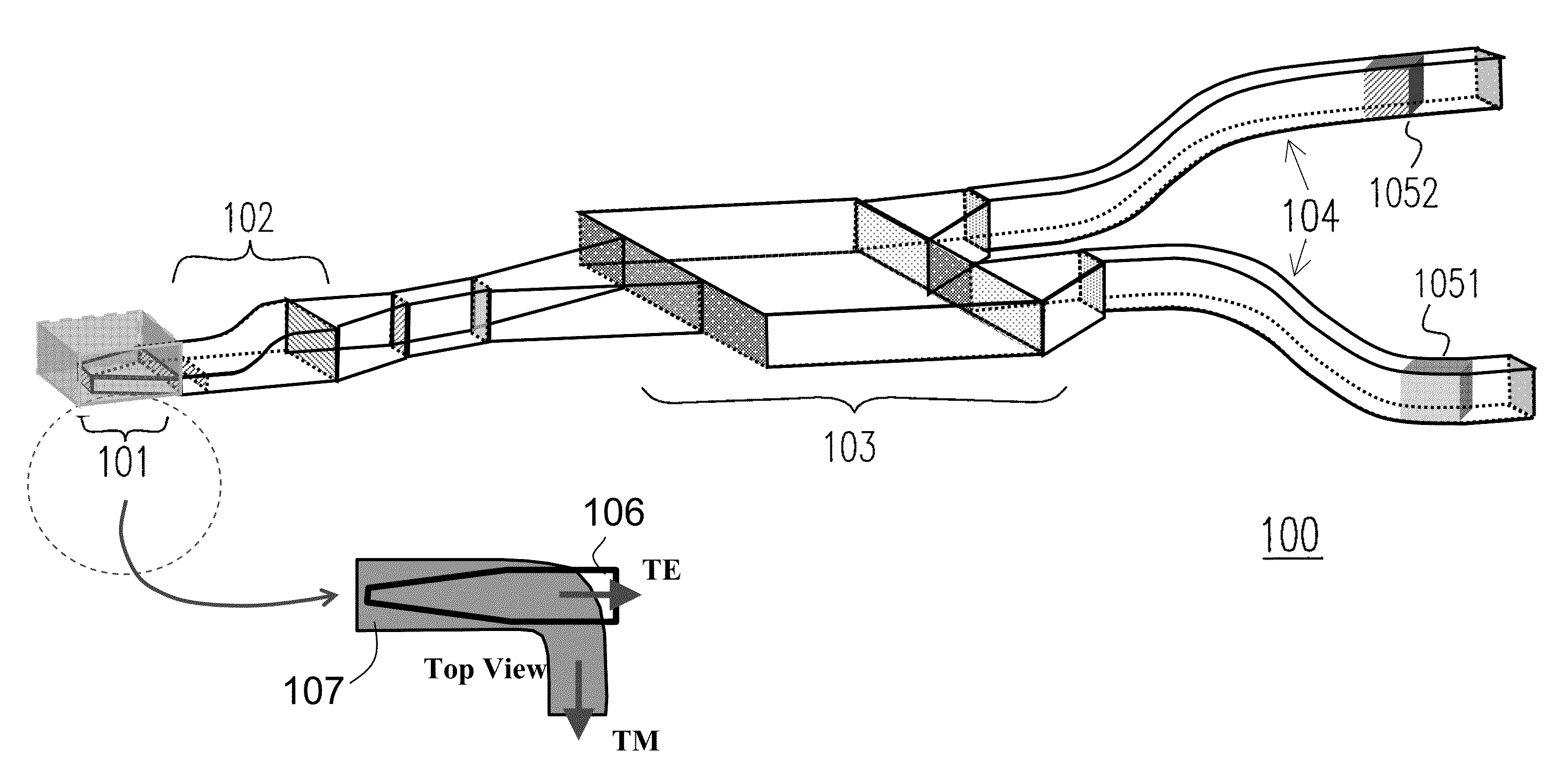
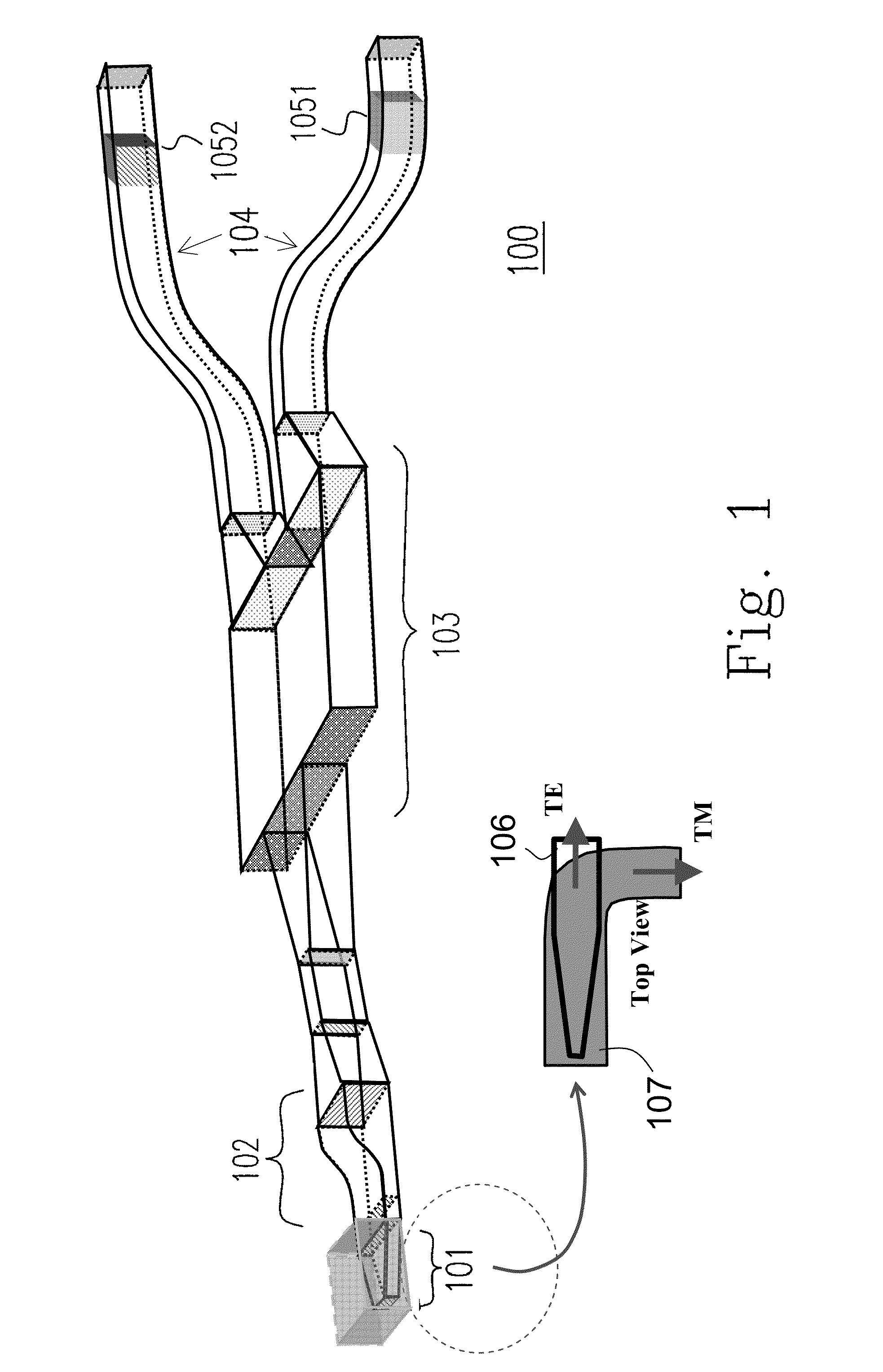
[0051]2. An optic chip as claimed in Embodiment 1 further comprising a bottom clad layer, wherein the waveguide, the top clad layer, and the bottom clad layer have a first, a second and a third refractive index respectively, the first refractive index is bigger than the second refractive index, and the second refractive index is bigger than the third refractive index.

embodiment 2

[0052]3. An optic chip as claimed in Embodiment 2, wherein the waveguide is a guiding layer made from the silicon, the top clad layer is the silicon carbide (SiC), and the bottom clad layer is the silicon dioxide.

[0053]4. An optic chip as claimed in Embodiment 1, wherein the waveguide is a taper waveguide.

embodiment 4

[0054]5. An optic chip as claimed in Embodiment 4, wherein the taper waveguide can guide one of the TE and TM electromagnetic waves to the output side of the polarization diversity coupler.

[0055]6. An optic chip as claimed in Embodiment 1, wherein the thicknesses of the waveguide and the top clad layer are obtained by FimmWave simulation or BPM simulation or the other simulation softwares.

[0056]7. An optic chip as claimed in Embodiment 1, wherein the top clad layer turns out the optic chip in 90 degree or any other bending angle adequate to reach the edge of the optic chip for outputting the unwanted polarized electromagnetic waves from the polarization diversity coupler.


PUM

PropertyMeasurementUnit
lengthaaaaaaaaaa
thickness A2aaaaaaaaaa

Abstract

This patent disclosure is based on silicon instead of LiNbO3, waveguide chip. The disclosed silicon-based multi-function integrated-optic chip comprises of unique design and fabrication features onto it. First, a unique polarization-diversity coupler is designed and fabricated to couple the external light into the silicon waveguide structure. Then TE mode is guided into a silicon slab waveguide, but TM mode is confined and diverted 90 degree in a silicon carbide structure till the chip edges for TM-mode suppression. Second, a unique two-step (vertical and lateral) taper waveguide region is designed and fabricated to bridge the polarization-diversity coupler output with the input of a multi-mode interferometer (MMI) splitter for power loss reduction. In this configuration, MMI may be a 1×2 or 2×2 structure to divide the input TE mode into a 50/50 splitting ratio output to form a Y-junction. Third, at either end of the Y-junction output, there is a phase modulator to achieve optical phase modulation through various physics mechanisms such as plasma dispersion, electro-optics, thermo-optics, or photo-elastic effect. With this newly-developed silicon-based multi-function integrated optic chip, the size and cost of fiber sensors including FOG's can be greatly reduced.

Description

FIELD OF THE INVENTION[0001]The invention relates to an optical chip, more particularly this invention is a silicon-based Multi-function Integrated-Optic Chip (MIOC) incorporates a unique polarization diversity coupler, and the two-step taper waveguide designs for single polarization, and low loss sensor applications. The silicon based waveguide is compatible with CMOS (Complementary Metal-Oxide Semiconductor) fabrication process, so integration of optical waveguide with electronic circuit in one chip is feasible that the size and cost of fiber sensors including Fiber-Optic Gyroscopes (FOG's) can be greatly reduced.BACKGROUND OF THE INVENTION[0002]Microminiaturization plays an increasingly imperative role in our daily life, especially for applications such as positioning, navigation and attitude control. Therefore, there is a need to develop highly integrated, sensitive and miniaturized gyroscopes to be incorporated as rotation sensors for the above mentioned applications.[0003]Amon...

Claims


Application Information

Patent Timeline
Patent Type & Authority Applications(United States)
IPC IPC(8): G02B6/26B23P11/00
CPCY10T29/49G02B6/26G02B6/2813Y10T29/49826G02B6/105
Inventor LEE, MING-CHANGLIU, REN-YOUNG
Owner TAIWAN SPACE AGENCY
Why Eureka
Try Eureka