Capacitive microelectronic and/or nanoelectronic device with increased compactness

a nanoelectronic and compact technology, applied in the direction of acceleration measurement using interia forces, instruments, coatings, etc., can solve the problems of air gap change, capacitance change between, and implies a substantial encumbrance in the plane, and achieve the effect of increasing the compactness in the plan

Active Publication Date: 2017-04-25
COMMISSARIAT A LENERGIE ATOMIQUE ET AUX ENERGIES ALTERNATIVES
View PDF15 Cites 1 Cited by
  • Summary
  • Abstract
  • Description
  • Claims
  • Application Information

AI Technical Summary

Benefits of technology

[0011]It is consequently a purpose of this invention to offer a capacitive device comprising a mobile portion and a fixed portion, offering an increased compactness in the plane.
[0016]Since the fixed and mobile electrodes are realised in a layer separate from that of the mobile element, the layer wherein the fixed and mobile electrodes are made can be advantageously thin while that of the mobile element can be thick. A thick mobile element makes it possible to reduce the footprint of the device in the plane at a constant level of precision. When the layer wherein the fixed and mobile electrodes are made is thin, it is possible to create a narrow air gap, for example less than 0.5 μm for a layer of 10 μm, the aspect ratio is then 20. A narrow air gap allows for substantial gains in electrical sensitivity, and to increase the density of the number of electrodes and to further increase the sensitivity.
[0017]Since the fixed and mobile electrodes are made using the same layer advantageously simultaneously, the air gap between the electrodes can be created via etching, which allows for good dimensional control of the air gaps.
[0021]Also advantageously, the capacitive means are of the interdigitated comb type, which makes it possible to increase the density of the number of electrodes.

Problems solved by technology

The relative movement of the seismic mass with respect to the substrate causes a relative movement between the interdigitated fingers, which results in an air gap change and a capacitance change between the fixed fingers with respect to the substrate and the fixed fingers with respect to the inertial mass.
This configuration implies a substantial encumbrance in the plane.
As the combs are arranged around the inertial mass, the footprint in the plane is even further substantial.
This results in a loss of electrical sensitivity of the component.
This results in a substantial air gap, for example much higher than 1 μm, which limits the electrical sensitivity.
Furthermore, this air gap is poorly controlled.

Method used


Image

  • Capacitive microelectronic and/or nanoelectronic device with increased compactness
  • Capacitive microelectronic and/or nanoelectronic device with increased compactness
  • Capacitive microelectronic and/or nanoelectronic device with increased compactness

Examples


Embodiment Construction

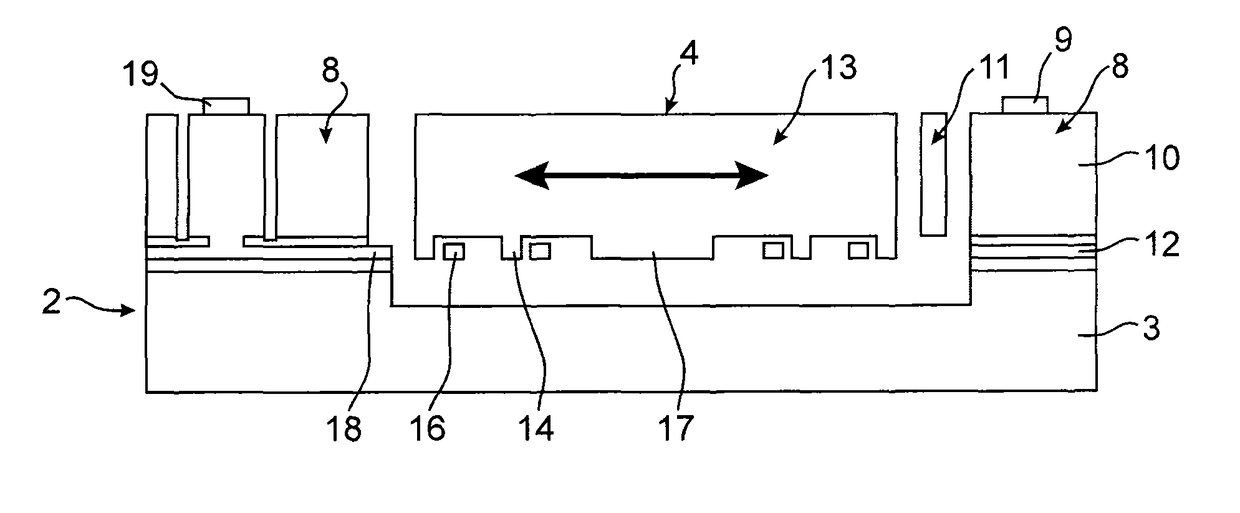
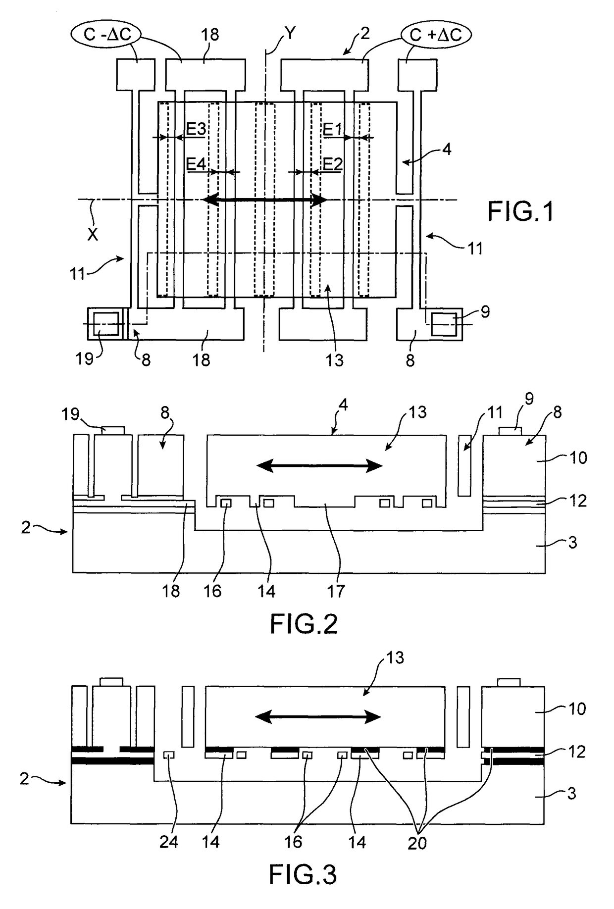
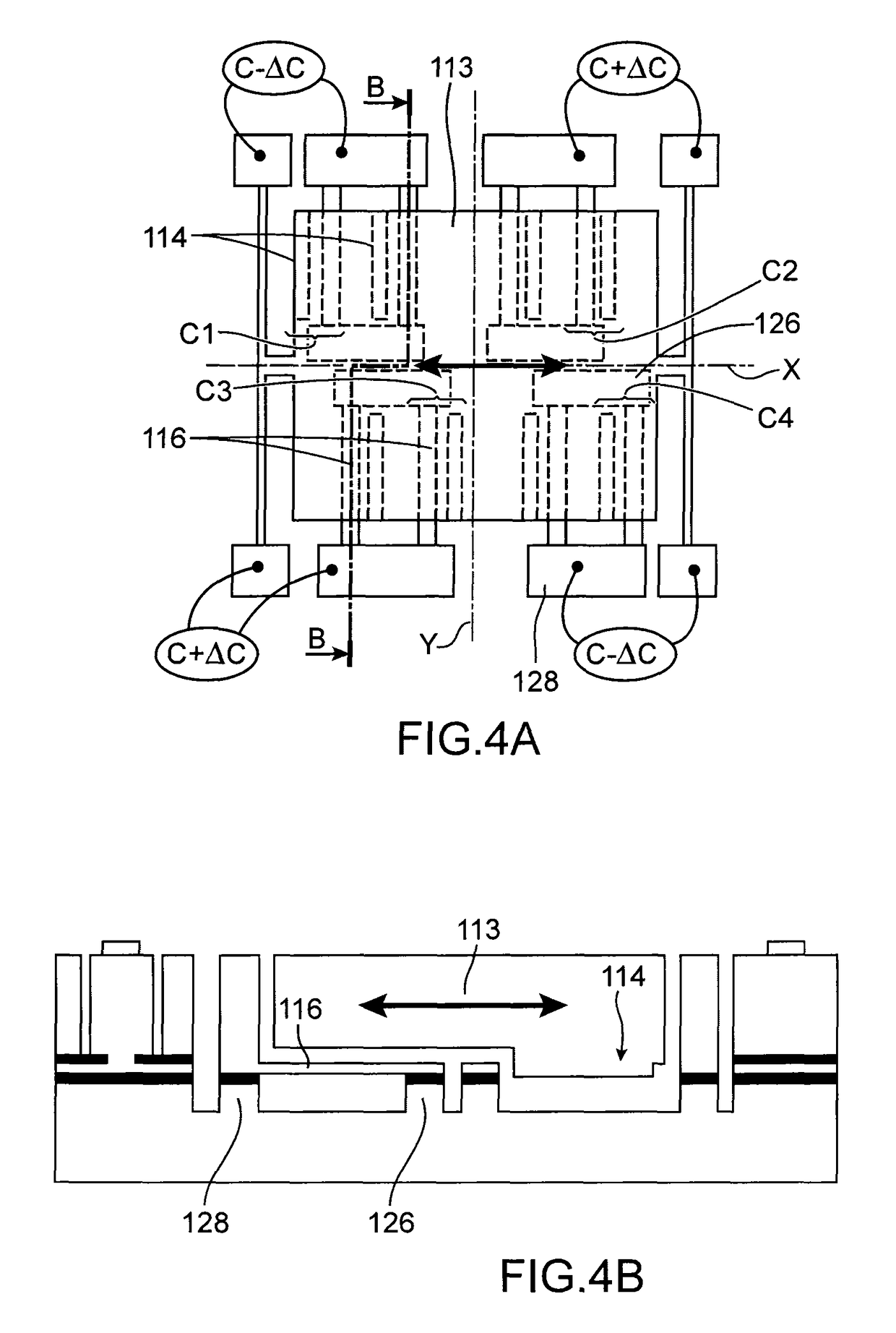
[0063]FIGS. 1 and 2 show an embodiment of a micro and / or nanoelectronic device with mobile element wherein a capacitance change is measured. For the purposes of simplicity, the latter will be designated solely as capacitive device in the remainder of the description. Moreover, in the following description the fixed or mobile electrodes are used for the purposes of measuring the movement of the mobile element, they shall then be designated as detection electrodes, but as shall be described in what follows, they can be used to actuate the mobile element, i.e. to set it into movement and / or to place it into a given position.

[0064]In the example of FIGS. 1 and 2, the capacitive device comprises a fixed portion 2 and a mobile portion 4. The mobile portion 4 is able to move with respect to the fixed portion 2 along a longitudinal direction X.

[0065]The fixed portion 2 comprises a support 3 for example formed using a semi-conductive substrate, for example made of silicon and detection elect...


PUM

PropertyMeasurementUnit
aspect ratioaaaaaaaaaa
thicknessaaaaaaaaaa
thicknessaaaaaaaaaa

Abstract

A device with a mobile element extending along a given plane comprising at least one first, one second and one third layers extending in planes parallel to the given plane, with the first layer forming a support, the second layer comprising all or a portion of the mobile element and means for suspending the mobile element with respect to the support and the third layer comprising all or a portion of the capacitive means of which the capacitance varies according to the relative position of the mobile element with respect to the support, said capacitive means comprising at least one mobile electrode integral with one of the faces of the mobile element parallel to the given plane, and at least one fixed electrode with respect to the support, with the fixed and mobile electrodes being arranged at least partially in the same plane parallel to the given plane and at least partially above and / or below the mobile element.

Description

TECHNICAL FIELD AND PRIOR ART[0001]This invention relates to a microelectronic and / or nanoelectronic device comprising a mobile portion and a fixed portion and capacitive means of which the capacitance varies with the relative movement of the mobile and fixed portions, with the device able to have increased compactness.[0002]The capacitance change due to the relative movement of the mobile and fixed portions can be used for the detection of the relative movement between a fixed portion and a mobile portion and is for example implemented in microelectromechanical or MEMS (MicroElectroMechanical System) systems used to realise sensors such as accelerometers, gyrometers, magnetometers.[0003]The uses of capacitive MEMS sensors are multiple. The latter are for example used in the automobile, in the general public field as for example in portable telephones, in electronic games, in aeronautics, the medical field, etc.[0004]It is sought not only to reduce the cost of the sensors but also t...

Claims


Application Information

Patent Timeline
Patent Type & Authority Patents(United States)
IPC IPC(8): H01G5/14B81B3/00G01P15/125B81C1/00H01G5/16G01D5/241G01P15/08
CPCB81B3/0021B81C1/00134G01D5/2417G01P15/125H01G5/14H01G5/16B81B2201/033B81B2203/051G01P2015/0814B81B2203/055
Inventor ROBERT, PHILIPPEJOET, LOIC
Owner COMMISSARIAT A LENERGIE ATOMIQUE ET AUX ENERGIES ALTERNATIVES
Why Eureka
Try Eureka