Fabrication of field-effect transistors with atomic layer doping

a technology of atomic layer doping and field-effect transistors, which is applied in the direction of transistors, semiconductor devices, electrical apparatus, etc., can solve the problems of increasing power consumption in idle state, inefficient planar fet transistors, and increasing inefficiency of the nanometer scale, so as to increase the conductivity of the semi-conducting surface

Inactive Publication Date: 2013-02-07
ALSEPHINA INNOVATIONS INC
View PDF4 Cites 7 Cited by
  • Summary
  • Abstract
  • Description
  • Claims
  • Application Information

AI Technical Summary

Benefits of technology

[0008]One embodiment is directed to an atomic layer doping method. In accordance with the method, a semiconducting surface and a dopant gas mixture are prepared. Further, a dopant layer is grown on the semiconducting surface by applying the dopant gas mixture to the semiconducting surface under a pressure that is less than 500 Torr and a temperature that is between 300° C. and 750° C. The dopant layer includes at least 4×10²⁰ active dopant atoms per cm3 that react with atoms on the semiconducting surface such that the reacted atoms increase the conductivity of the semiconducting surface.
[0010]An alternative embodiment is directed to a multigate field-effect transistor device. The device includes a gate structure and at least one fin. The gate structure envelopes a plurality of surfaces of one or more fins, which are above a substrate. The fin provides a channel between a source and the gate structure and between a drain and the gate structure. In addition, the fin is composed of a semiconducting material and a dopant layer that conformally overlays the semiconducting material in three-dimensions. Further, the dopant layer includes at least 4×10²⁰ active dopant atoms per cm3 that are bonded with atoms on a surface of the semiconducting material such that bonding between the active dopant atoms and the atoms on the surface of the semiconducting material increases the conductivity of the surface of the semiconducting material.

Problems solved by technology

Planar FET transistors, which have been widely used in integrated circuits for the past several decades, were found to be increasingly inefficient on the nanometer scale.
Reducing the size of the channel between the terminals of planar transistors to this scale leads to an inefficient leakage of current in the off-state of the transistor, resulting in an increase in power consumption in its idle state.

Method used


Image

  • Fabrication of field-effect transistors with atomic layer doping
  • Fabrication of field-effect transistors with atomic layer doping
  • Fabrication of field-effect transistors with atomic layer doping

Examples


Embodiment Construction

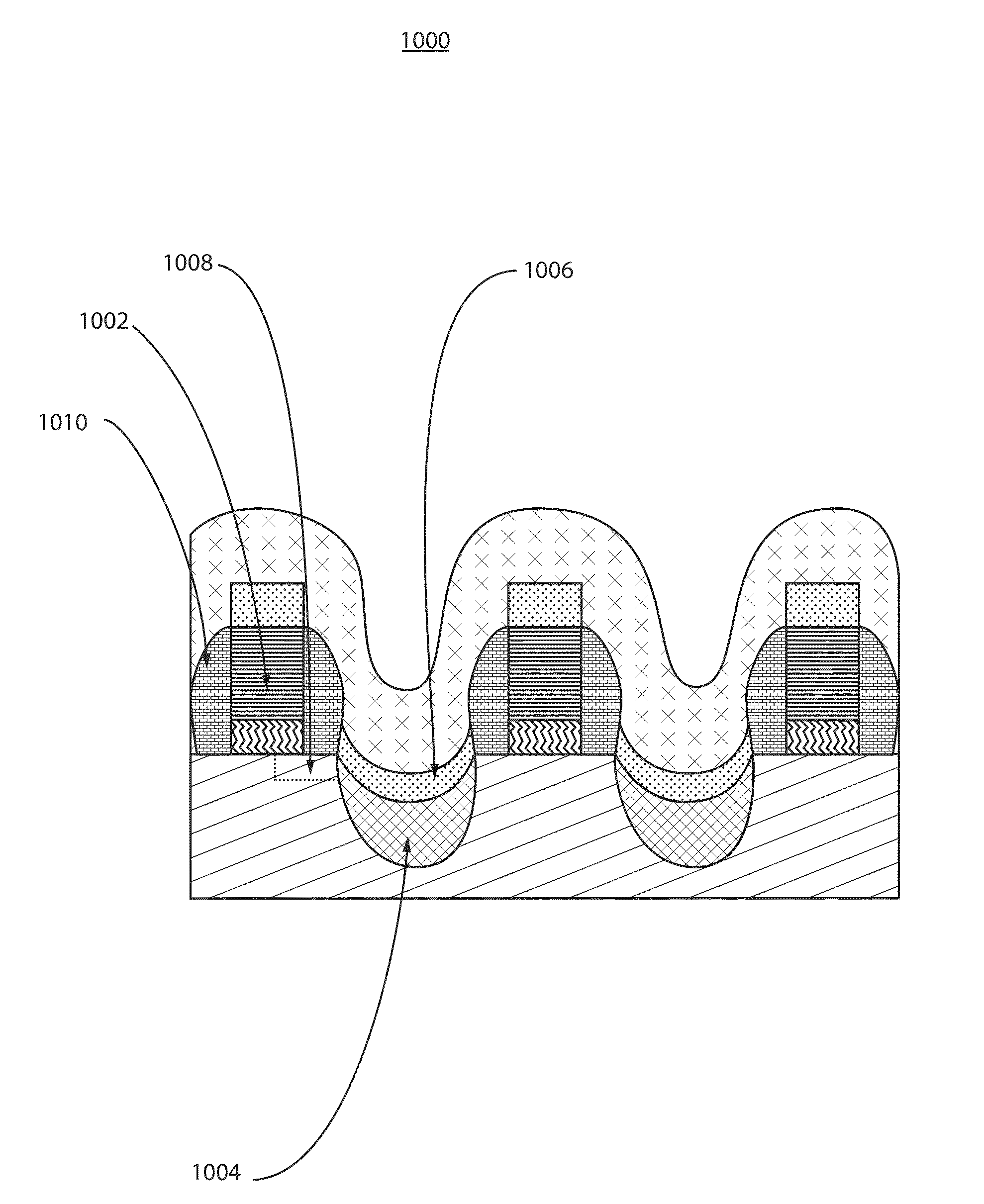
[0023]One of the most important problems in scaling down complementary metal-oxide semiconductor (CMOS) transistors is the ability to control transistor leakage current (Ioff) while increasing the drive current (Ion). Fully depleted devices, such as extremely thin silicon on insulator (ETSOI) field-effect transistors (FET), Trigate transistors and FinFETs, which can have a sub-threshold slope approaching a theoretical value of 60 mV / dec, may be good candidates to address the problem. While these devices offer excellent short channel effect (SCE) control, they suffer from high extension resistance that degrades the transistor performance.

[0024]For example, Trigate and FinFET transistor extensions are typically fabricated by performing ion implantation of either n or p-dopants. However, ion implants amorphorize the silicon fin. In addition, the fin cannot be re-crystallized by rapid thermal anneal due to the small, available silicon seed surface area. Thus, the device is formed with a...


PUM

PropertyMeasurementUnit
thicknessaaaaaaaaaa
temperatureaaaaaaaaaa

Abstract

Field effect transistors fabricated using atomic layer doping processes are disclosed. In accordance with an embodiment of an atomic layer doping method, a semiconducting surface and a dopant gas mixture are prepared. Further, a dopant layer is grown on the semiconducting surface by applying the dopant gas mixture to the semiconducting surface under a pressure that is less than 500 Torr and a temperature that is between 300° C. and 750° C. The dopant layer includes at least 4×10²⁰ active dopant atoms per cm3 that react with atoms on the semiconducting surface such that the reacted atoms increase the conductivity of the semiconducting surface.

Description

[0001]RELATED APPLICATION DATA[0002]This application is a Continuation application of co-pending U.S. patent application Ser. No. 13 / 198,255 filed on Aug. 4, 2011, incorporated herein by reference in its entirety.BACKGROUND[0003]1. Technical Field[0004]The present invention relates to semiconductor devices, and more particularly, to devices and fabrication methods that utilize atomic layer doping techniques.[0005]2. Description of the Related Art[0006]Throughout the evolution and advancement of computing devices, reducing their size and their power consumption while maintaining a high processing capacity have long been design goals. Transistors have been the cornerstone of electrical circuits of computing devices. A common transistor type is field-effect transistors (FET), in which the conductivity of a channel between terminals of the transistor is dependent on electric fields. Basic elements of an FET include a gate, a source and a drain, which are connected to conductive lines th...

Claims


Application Information

Patent Timeline
Patent Type & Authority Applications(United States)
IPC IPC(8): H01L29/78
CPCH01L21/2254H01L29/665H01L29/6653H01L29/6659H01L29/66636H01L29/7833H01L29/7848H01L29/785H01L29/165H01L21/0228H01L29/365H01L29/66803H01L21/3141H01L21/31H01L21/2252H01L21/324H01L29/0847H01L29/45
Inventor CHAN, KEVIN K.KIM, YOUNG-HEELAUER, ISAACMURALIDHAR, RAMACHANDRANPARK, DAE-GYUWANG, XINHUIYANG, MIN
Owner ALSEPHINA INNOVATIONS INC
Why Eureka
Try Eureka