Probing device

a technology of probes and probes, applied in measurement devices, electrical testing, instruments, etc., can solve the problems of increased overdrive needs, increased wear, and inevitable defects of chips, and achieve the effect of adequate flatness and longer service li

Active Publication Date: 2013-02-07
MICROELECTRONICS TECH INC
View PDF1 Cites 7 Cited by
  • Summary
  • Abstract
  • Description
  • Claims
  • Application Information

AI Technical Summary

Benefits of technology

[0009]The main objective of the present invention is to provide a probing device which can avoid a space transformer from deformation while pressed.
[0023]Due to the displacement of the reinforcing plate, the space transformer does not deform while pressed. Therefore, the space transformer can have adequate flatness, which contributes to a longer service life of the space transformer and the probes.

Problems solved by technology

Due to the complication of the manufacturing process, some chips are inevitably defective.
The worse the flatness of the probe card is, the bigger the over drive needs to be.
However, such a bigger amount of force results in more serious deformation of the space transformer 14 and more wear to the probes 162 themselves, thereby shortening the service life of the space transformer 14 and the probes 162.

Method used


Image

  • Probing device
  • Probing device
  • Probing device

Examples


first embodiment

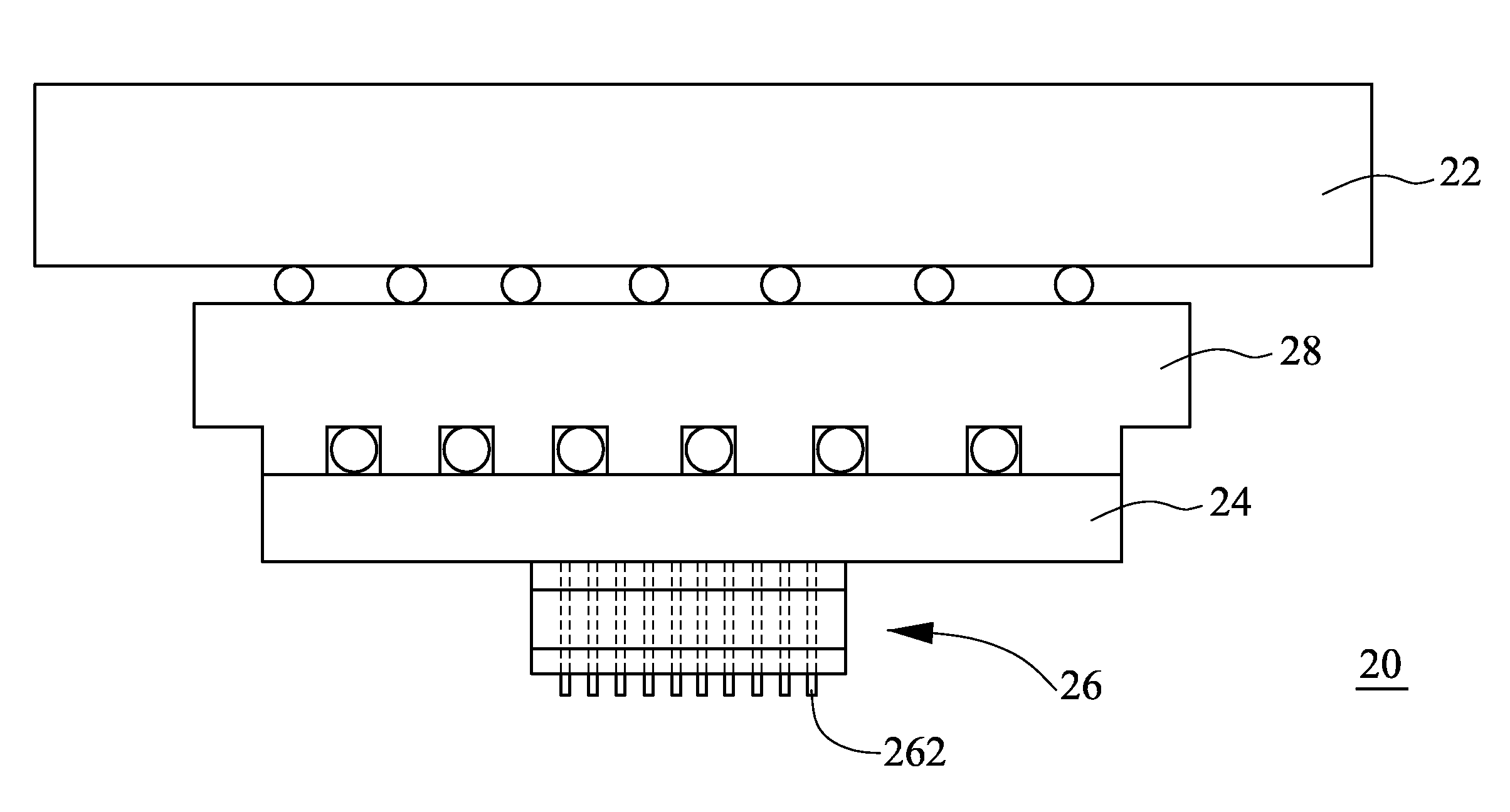
[0039]Please refer to FIG. 2A for a probing device of the present invention. The probing device 20 includes a circuit board 22, a reinforcing plate 28, a space transformer 24, and a probe assembly 26. The reinforcing plate 28 is disposed on a side of the circuit board 22, and the reinforcing plate 28 has a plurality of inner conductive wires (not shown) electrically connecting to those of the circuit board 22. The reinforcing plate 28 is a multi-layered ceramic (MLC) structure. Due to the higher hardness of ceramic, the probing device 20 as a whole has better mechanical strength. Moreover, the space transformer 24 is disposed on the reinforcing plate 28, and the space transformer 24 has a plurality of inner conductive wires electrically connecting to those of the reinforcing plate 28. The space transformer 24 is a multi-layered organic structure. Furthermore, the probe assembly 26 includes a plurality of probes 262, and the probe assembly 26 is disposed on the space transformer 24.

[...

second embodiment

[0043]In the above embodiment, the protrusions 283 are protruded from the reinforcing plate 28 to support the space transformer 24. However, such characteristic is not always necessary. The protrusions 283, for example, can also be formed on the space transformer 24. Referring to FIG. 3, a probing device of the present invention is shown. In the present embodiment, the reinforcing plate 48 is planar, and the space transformer 44 has a plurality of protrusions 443. These protrusions 443 are adapted to abut against the reinforcing plate 48 and define a plurality of receiving spaces 442 therebetween for receiving the first solder balls 441.

third embodiment

[0044]Furthermore, the protrusions can also be formed both on the reinforcing plate and the space transformer. Please refer to FIG. 4 for a probing device of the present invention. The reinforcing plate 58 has a plurality of first protrusions 583, and the space transformer 54, on the other hand, has a plurality of second protrusions 543 abutting against the first protrusions 583. A plurality of receiving spaces 582 are defined between the first protrusions 583 and the second protrusions 543 for receiving first solder balls 541.

[0045]In the second and third embodiments, the protrusion 443, the first protrusion 583, and the second protrusion 543 are formed, for example, in the manner of lithography. More specifically, a photoresist layer (not shown) is coated on the reinforcing plate 58 or the space transformer 54. The photoresist layer is then patterned to form the protrusions. In other words, the protrusions are made of photoresist. The protrusion 443, the first protrusion 583 and t...


PUM


Abstract

A probing device includes a circuit board, a reinforcing plate, at least one space transformer and at least one probe assembly. The reinforcing plate is disposed on the circuit board, and the reinforcing plate has a plurality of inner conductive wires electrically connecting to those of the circuit board. The reinforcing plate defines a plurality of receiving space therein. The space transformer is disposed on the reinforcing plate, and the space transformer has a plurality of inner conductive wires electrically connecting to those of the reinforcing plate via a plurality of first solder balls. The probe assembly is disposed on the space transformer, and the probe assembly includes a plurality of probes. The first solder balls are disposed in the receiving spaces, and the reinforcing plate abuts against the space transformer.

Description

FIELD OF THE INVENTION[0001]The present invention relates to a testing device, and more particularly to a probing device for wafer-level testing.BACKGROUND[0002]It typically involves many steps, including lithography, deposition, etching and etc., to form a plurality of integrated circuit (IC) chips on a wafer. Due to the complication of the manufacturing process, some chips are inevitably defective. Therefore, the chips are tested for functional defects before the wafer is sent to dicing preparation.[0003]Please refer to FIG. 1A, which shows a conventional probing device 10. The conventional probing device 10 includes a circuit board 12, a space transformer 14, and a probe assembly 16. The space transformer 14 is disposed on the circuit board 12 with an interface composed of a plurality of solder balls 142. The probe assembly 16 is disposed on the space transformer 14 and has a plurality of probes 162, by which the chips on the wafer are tested. Conductive wires (not shown) within ...

Claims


Application Information

Patent Timeline
Patent Type & Authority Applications(United States)
IPC IPC(8): G01R31/00
CPCG01R1/07378G01R1/07342
Inventor WU, CHIEN-CHOUCHEN, MING-CHILI, CHUNG-CHE
Owner MICROELECTRONICS TECH INC
Why Eureka
Try Eureka