Method of fabricating resistance variable memory device and devices and systems formed thereby

Inactive Publication Date: 2013-02-14
SAMSUNG ELECTRONICS CO LTD
View PDF28 Cites 21 Cited by
  • Summary
  • Abstract
  • Description
  • Claims
  • Application Information

AI Technical Summary

Benefits of technology

[0005]Other exemplary embodiments in accordance with principles of inventive concepts p

Problems solved by technology

However, as device densities increase, equipment a

Method used


Image

  • Method of fabricating resistance variable memory device and devices and systems formed thereby
  • Method of fabricating resistance variable memory device and devices and systems formed thereby
  • Method of fabricating resistance variable memory device and devices and systems formed thereby

Examples


example exemplary embodiments

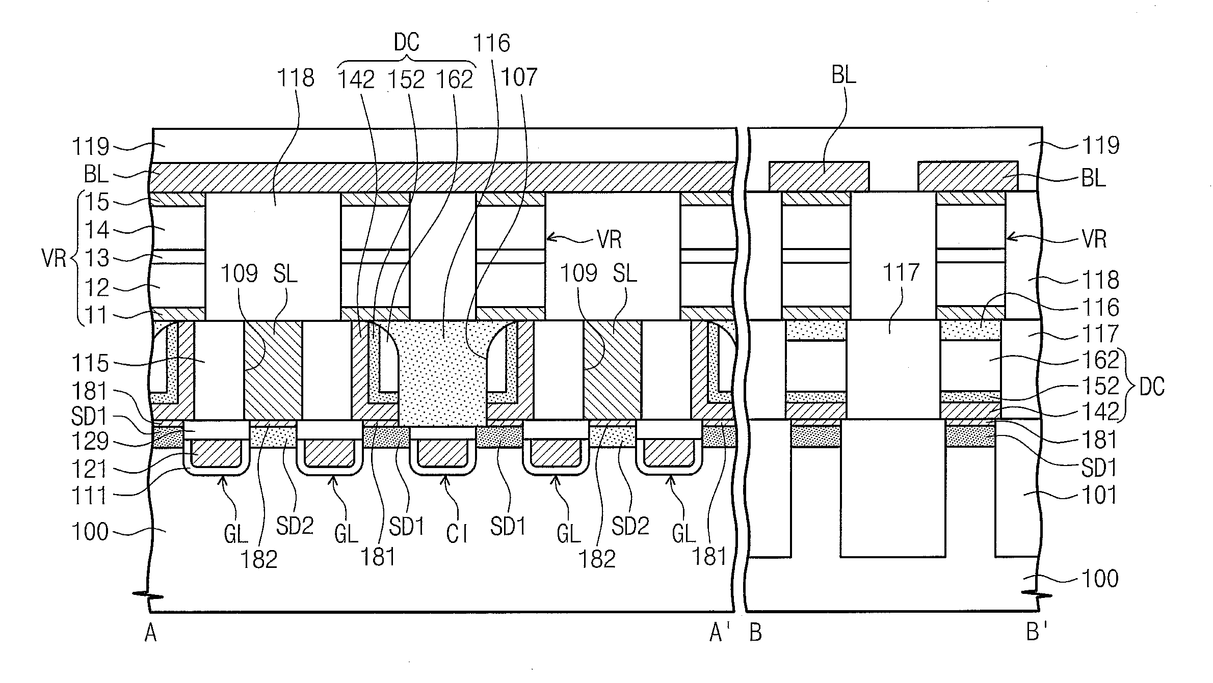
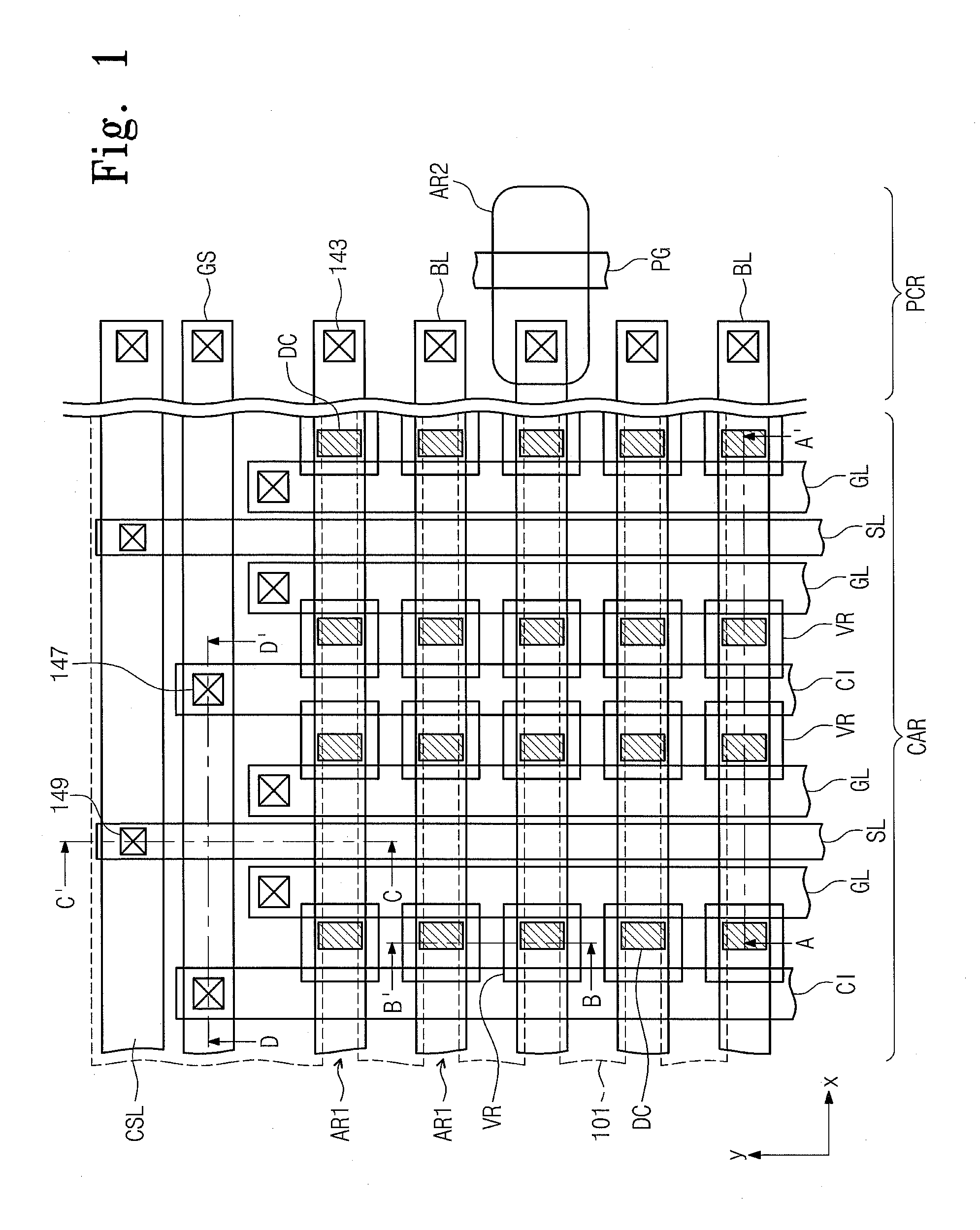
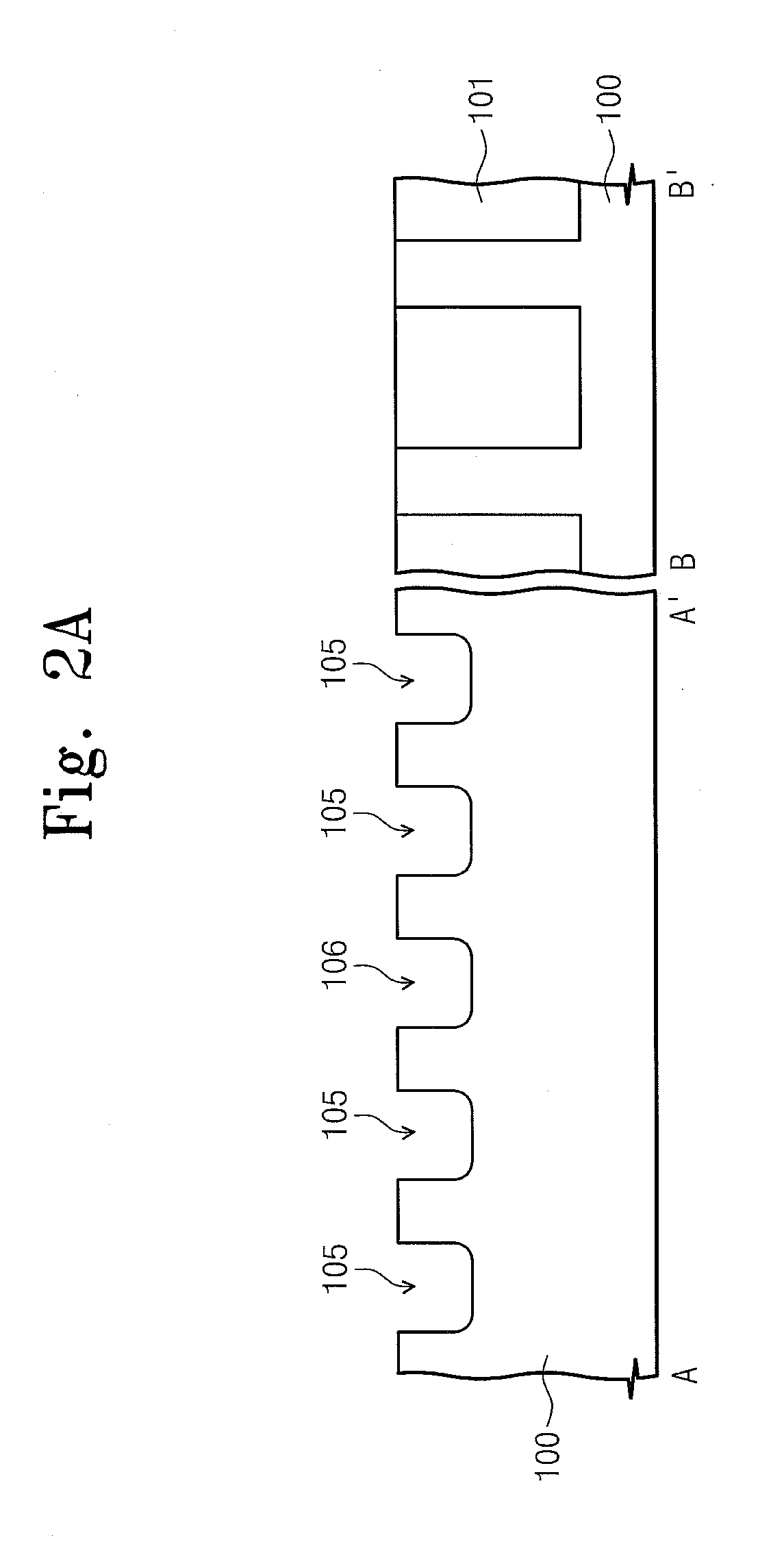
[0044 in accordance with principles of inventive concepts are described herein with reference to cross-sectional illustrations that are schematic illustrations of idealized embodiments (and intermediate structures) of example embodiments. As such, variations from the shapes of the illustrations as a result, for example, of manufacturing techniques and / or tolerances, are to be expected. Thus, example exemplary embodiments in accordance with principles of inventive concepts should not be construed as limited to the particular shapes of regions illustrated herein but are to include deviations in shapes that result, for example, from manufacturing. For example, an implanted region illustrated as a rectangle may have rounded or curved features and / or a gradient of implant concentration at its edges rather than a binary change from implanted to non-implanted region. Likewise, a buried region foimed by implantation may result in some implantation in the region between the buried region and...


PUM


Abstract

An exemplary method of forming a variable resistance memory may include forming first source/drain regions in a substrate, forming gate line structures and conductive isolation patterns buried in the substrate with the first source/drain regions interposed therebetween, and forming lower contact plugs on the first source/drain regions. The forming of lower contact plugs may include forming a first interlayer insulating layer, including a first recess region exposing the first source/drain regions adjacent to each other in a first direction, forming a conductive layer in the first recess region, patterning the conductive layer to form preliminary conductive patterns spaced apart from each other in the first direction, and patterning the preliminary conductive patterns to form conductive patterns spaced apart from each other in a second direction substantially orthogonal to the first direction.

Description

CROSS-REFERENCE TO RELATED APPLICATIONS[0001]This U.S. non-provisional patent application claims priority under 35 U.S.C. §119 to Korean Patent Application No. 10-2011-0080214, filed on Aug. 11, 2011, in the Korean Intellectual Property Office, the entire contents of which are hereby incorporated by reference.BACKGROUND OF THE INVENTION[0002]Exemplary embodiments in accordance with principles of inventive concepts relate generally to semiconductor devices, and more particularly, to variable resistance memory devices and methods of fabricating the same.[0003]For decades, electronic devices have steadily increased their performance and reliability, at least in part, by reducing the size of features in their circuits and thereby dramatically increasing device density. Memory devices are often at the vanguard of improvements in device density. However, as device densities increase, equipment and facility costs increase at an accelerating rate. A system and method that enables increases ...

Claims


Application Information

Patent Timeline
IPC IPC(8): H01L21/8239
CPCH01L21/76897H01L27/2436H01L27/228H10B63/30H10B61/22H10N70/20
Inventor NAM, KYUNGTAEKIM, KI JOONHWANG, YOUNGNAM
Owner SAMSUNG ELECTRONICS CO LTD
Why Eureka
Try Eureka