Methods for fabricating finfet integrated circuits in bulk semiconductor substrates

a technology of integrated circuits and semiconductor substrates, applied in the direction of semiconductor devices, electrical apparatus, nanotechnology, etc., can solve the problems of planarization and etch processing steps, non-uniform channel width and finfet characteristics,

Active Publication Date: 2013-02-21
TESSERA ADVANCED TECH
View PDF2 Cites 57 Cited by
  • Summary
  • Abstract
  • Description
  • Claims
  • Application Information

AI Technical Summary

Benefits of technology

[0006]Methods are provided for fabricating FinFETs that avoid thickness uniformity problems across a die or a substrate. One embodiment includes providing a semiconductor substrate divided into a plurality of chips, each chip bounded by scribe lines. The substrate is etched to form a plurality of fins, each of the fins extending uniformly across the width of the chips. An oxide is deposited to fill between the fins and is et...

Problems solved by technology

One of those problems involves isolation between adjacent fins and between adjacent active areas.
The combination of the two types of isolation trenches, one shallow, narrow and dense, the other...

Method used


Image

  • Methods for fabricating finfet integrated circuits in bulk semiconductor substrates
  • Methods for fabricating finfet integrated circuits in bulk semiconductor substrates
  • Methods for fabricating finfet integrated circuits in bulk semiconductor substrates

Examples


Embodiment Construction

[0013]The following detailed description is merely exemplary in nature and is not intended to limit the invention or the application and uses of the invention. Furthermore, there is no intention to be bound by any expressed or implied theory presented in the preceding technical field, background, brief summary or the following detailed description.

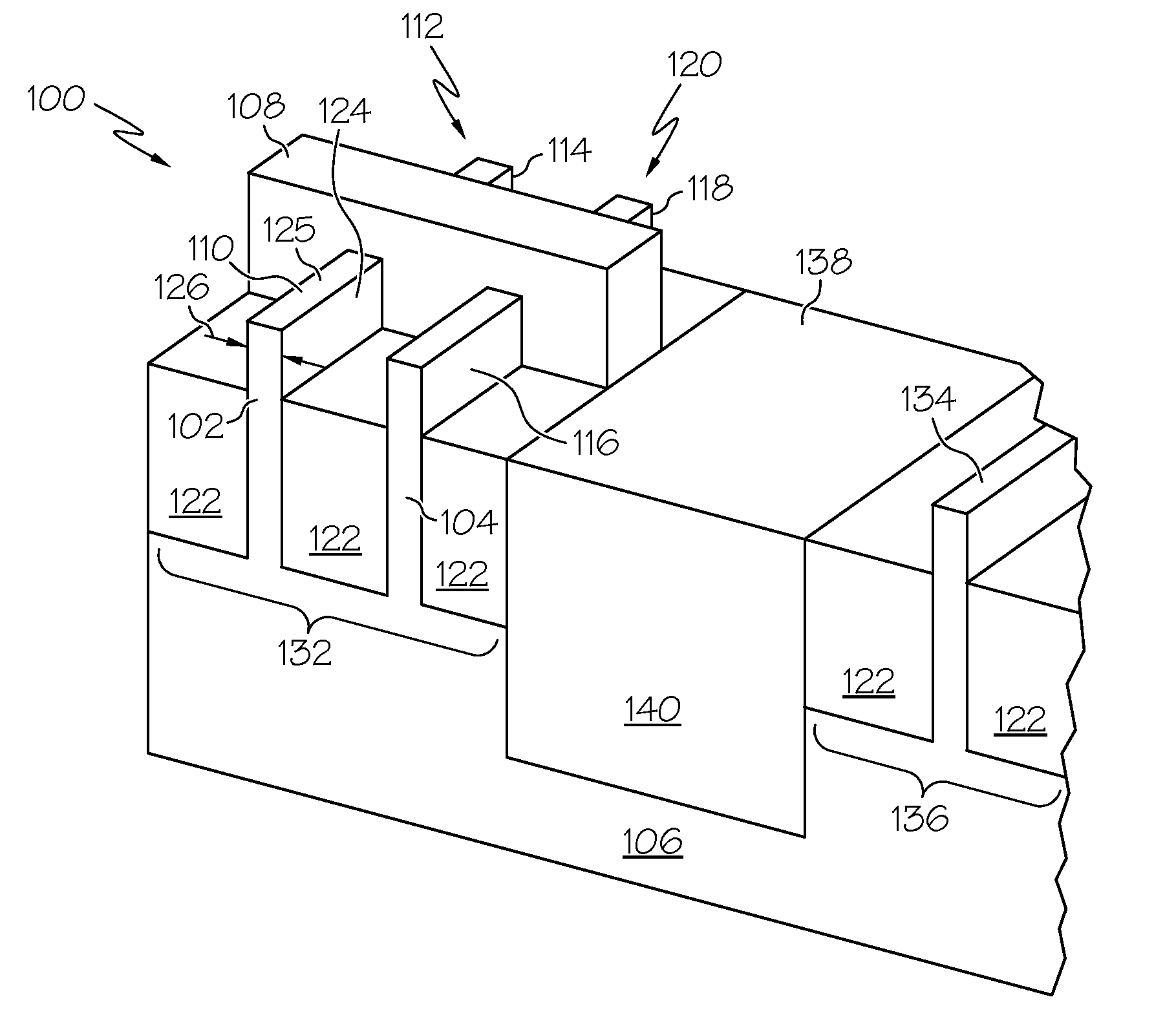
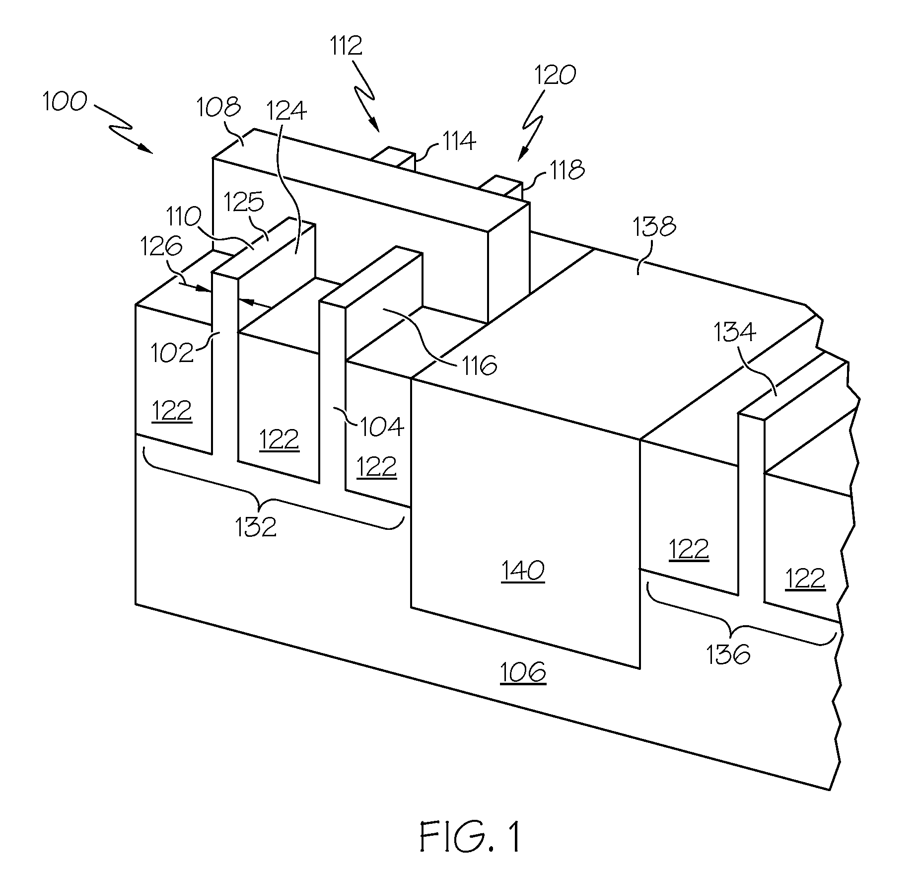
[0014]FIG. 1 illustrates, in a cut away perspective view, a portion of a FinFET integrated circuit (IC) 100. The illustrated portion of IC 100 includes two fins 102 and 104 that are formed from and extend upwardly from a bulk semiconductor substrate 106. Fins 102 and 104 are located in active area 132. A gate electrode 108 overlies the two fins and is electrically insulated from the fins by a gate insulator (not illustrated). End 110 of fin 102 is appropriately impurity doped to form the source of a FinFET 112 and end 114 of that fin is appropriately impurity doped to form the drain of the FinFET. Similarly, ends 116 and 118 of fin 104 for...


PUM


Abstract

Methods are provided for fabricating FinFETs that avoid thickness uniformity problems across a die or a substrate. One method includes providing a semiconductor substrate divided into a plurality of chips, each chip bounded by scribe lines. The substrate is etched to form a plurality of fins, each of the fins extending uniformly across the width of the chips. An oxide is deposited to fill between the fins and is etched to recess the top of the oxide below the top of the fins. An isolation hard mask is deposited and patterned overlying the plurality of fins and is used as an etch mask to etch trenches in the substrate defining a plurality of active areas, each of the plurality of active areas including at least a portion of at least one of the fins. The trenches are filled with an insulating material to isolate between adjacent active areas.

Description

TECHNICAL FIELD[0001]The present invention generally relates to methods for fabricating integrated circuits, and more particularly relates to methods for manufacturing FinFET integrated circuits in bulk semiconductor substrates that avoid thickness uniformity problems.BACKGROUND[0002]Transistors such as metal oxide semiconductor field effect transistors (MOSFETs) or simply field effect transistors (FETs) are the core building blocks of the vast majority of semiconductor integrated circuits (ICs). A FET includes source and drain regions between which a current can flow through a channel under the influence of a bias applied to a gate electrode that overlies the channel. Some semiconductor ICs, such as high performance microprocessors, can include millions of FETs. For such ICs, decreasing transistor size and thus increasing transistor density has traditionally been a high priority in the semiconductor manufacturing industry. Transistor performance, however, must be maintained even as...

Claims


Application Information

Patent Timeline
IPC IPC(8): H01L21/336H01L21/762B82Y40/00
CPCH01L21/823431H01L21/76224H01L29/66545
Inventor CHO, JIN
Owner TESSERA ADVANCED TECH
Why Eureka
Try Eureka