Display panel, display device, and method of driving the same

Inactive Publication Date: 2013-03-07
SHARP KK
View PDF7 Cites 12 Cited by
  • Summary
  • Abstract
  • Description
  • Claims
  • Application Information

AI Technical Summary

Benefits of technology

The present invention relates to a display device with improved cost and current consumption. The technical effects of the invention include a decrease in the number of data signal lines, a reduction in the number of circuits in the data signal line drive circuit, and a decrease in picture-frame areas. The invention also includes a precharge operation to prevent charge shortage and a line inversion to suppress degradation of display quality. Additionally, the invention allows for a longer cycle of polarity inversion of data signals and decreases power consumption. Overall, the invention decreases the cost and current consumption of the display device.

Problems solved by technology

Therefore, cost of the data signal line drive circuit is higher than cost of the scanning signal line drive circuit.
Consequently, the cost of the data signal line drive circuit becomes higher, and at the same time, current consumption increases.
That is, when the number of data signal lines increases, cost and current consumption of the display device as a whole increase.
Because the number of the data signal lines increases in proportion to the number of pixel formation portions, the above problem becomes serious when sizes of display devices are progressively increased in recent years.

Method used


Image

  • Display panel, display device, and method of driving the same
  • Display panel, display device, and method of driving the same
  • Display panel, display device, and method of driving the same

Examples


first embodiment

1. First Embodiment

1.1 Entire Configuration

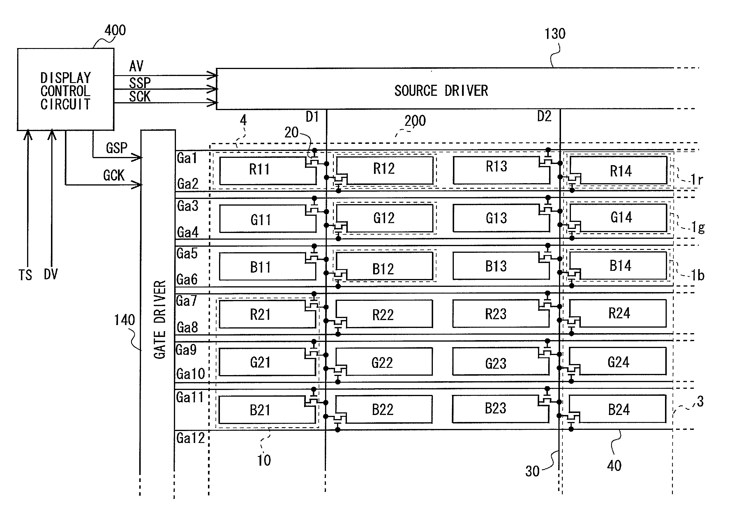
[0100]FIG. 1 is a pattern diagram showing an electrical configuration of a liquid crystal display device according to a first embodiment of the present invention. This liquid crystal display device includes a liquid crystal panel 300 as a display panel, a source driver 130 as a data signal line drive circuit, and a gate driver 140 as a scanning signal line drive circuit. The source driver 130 and the gate driver 140 are connected to a display control circuit 400. An image signal DV for displaying a color image and a timing control signal TS are inputted to the display control circuit 400 from outside of the device. The liquid crystal panel 300 includes a plurality of data signal lines 30 connected to the source driver 130, and a plurality of scanning signal lines 40 connected to the gate driver 140. The plurality of data signal lines 30 and the plurality of scanning signal lines 40 are arranged so as to cross each other. The liquid crystal ...

second embodiment

2. Second Embodiment

[0124]Next, a liquid crystal display device according to a second embodiment of the present invention will be described. The liquid crystal display device according to the present embodiment has a configuration basically similar to that in the first embodiment, except that an inversion driving system and the scanning signals Ga1, Ga2, . . . are different from those in the first embodiment. In the following, these differences will be mainly described, and detailed descriptions of other points will be omitted by affixing the same reference characters to the same or corresponding portions.

[0125]FIG. 15(A) to FIG. 15(C) are transition diagrams showing an inversion driving method in the present embodiment. FIG. 15(A), FIG. 15(B), and FIG. 15(C) show polarities of data signals Dk taken into sub-pixel formation portions Xij in an n-th frame, an (n+1)-th frame, and an (n+2)-th frame, respectively. Each element in a matrix corresponds to a sub-pixel formation portion Xij....


PUM


Abstract

The present invention provides a display panel having decreased cost and current consumption by decreasing the number of data signal lines from the conventional number, a display device including the display panel, and a method of driving the display device.Each pixel formation portion (10) included in a display unit (200) of a display device is configured to arrange three sub-pixel formation portions (1r, 1g, 1b) for forming sub-pixels of mutually different color components in a data signal line extension direction. Each one data signal line (30) is arranged between a sub-pixel formation portion vertical string (3) in an odd-order from a front of a scanning signal line extension direction and a sub-pixel formation portion vertical string (3) adjacent to the sub-pixel formation portion vertical string (3) at the back of the scanning signal line extension direction. Sub-pixel formation portion vertical strings (3, 3) positioned at both sides of each data signal line (30) are connected to the data signal line. Each one scanning signal line (40) is arranged at both sides of a sub-pixel formation portion in a data signal line extension direction. Mutually adjacent sub-pixel formation portion vertical strings (3, 3) are connected to mutually different scanning signal line (40).

Description

TECHNICAL FIELD[0001]The present invention relates to an active matrix-type display panel, a display device including the same, and a method of driving the same.BACKGROUND ART[0002]In general, a display unit of a display panel in an active matrix-type display device is configured by a pixel formation portion laid out in a matrix form. This pixel formation portion has a plurality of sub-pixel formation portions. For example, in an active matrix-type display device that displays a color image based on three primary colors of R (red), G (green), and B (blue), one pixel formation portion is conventionally configured by arrangement of three sub-pixel formation portions for forming three sub-pixels of R, G, and B in a direction in which scanning signal lines extend. FIG. 18 is a pattern diagram showing an electrical configuration of relevant portions of this conventional active matrix-type display device. This display device includes a display unit 200, a data signal line drive circuit 13...

Claims


Application Information

Patent Timeline
IPC IPC(8): G09G5/10
CPCG02F1/136286G09G3/3614G09G2300/0439G09G2300/0426G09G3/3648
Inventor IWAMOTO, AKIHISAMORII, HIDEKIMIZUNAGA, TAKAYUKIIKUTA, KEI
Owner SHARP KK
Why Eureka
Try Eureka