Electro-optice device comprising a ridge waveguide and a PN junction and method of manufacturing said device

Active Publication Date: 2013-03-07
POINTCLOUD INC
View PDF7 Cites 37 Cited by
  • Summary
  • Abstract
  • Description
  • Claims
  • Application Information

AI Technical Summary

Benefits of technology

[0019]Thus according to embodiments of the present invention a mask may be used to define a waveguide rib, and also as part of a barrier for doping a region adjacent to the waveguide rib. The fa

Problems solved by technology

This will decrease device performance variatio

Method used


Image

  • Electro-optice device comprising a ridge waveguide and a PN junction and method of manufacturing said device
  • Electro-optice device comprising a ridge waveguide and a PN junction and method of manufacturing said device
  • Electro-optice device comprising a ridge waveguide and a PN junction and method of manufacturing said device

Examples


Embodiment Construction

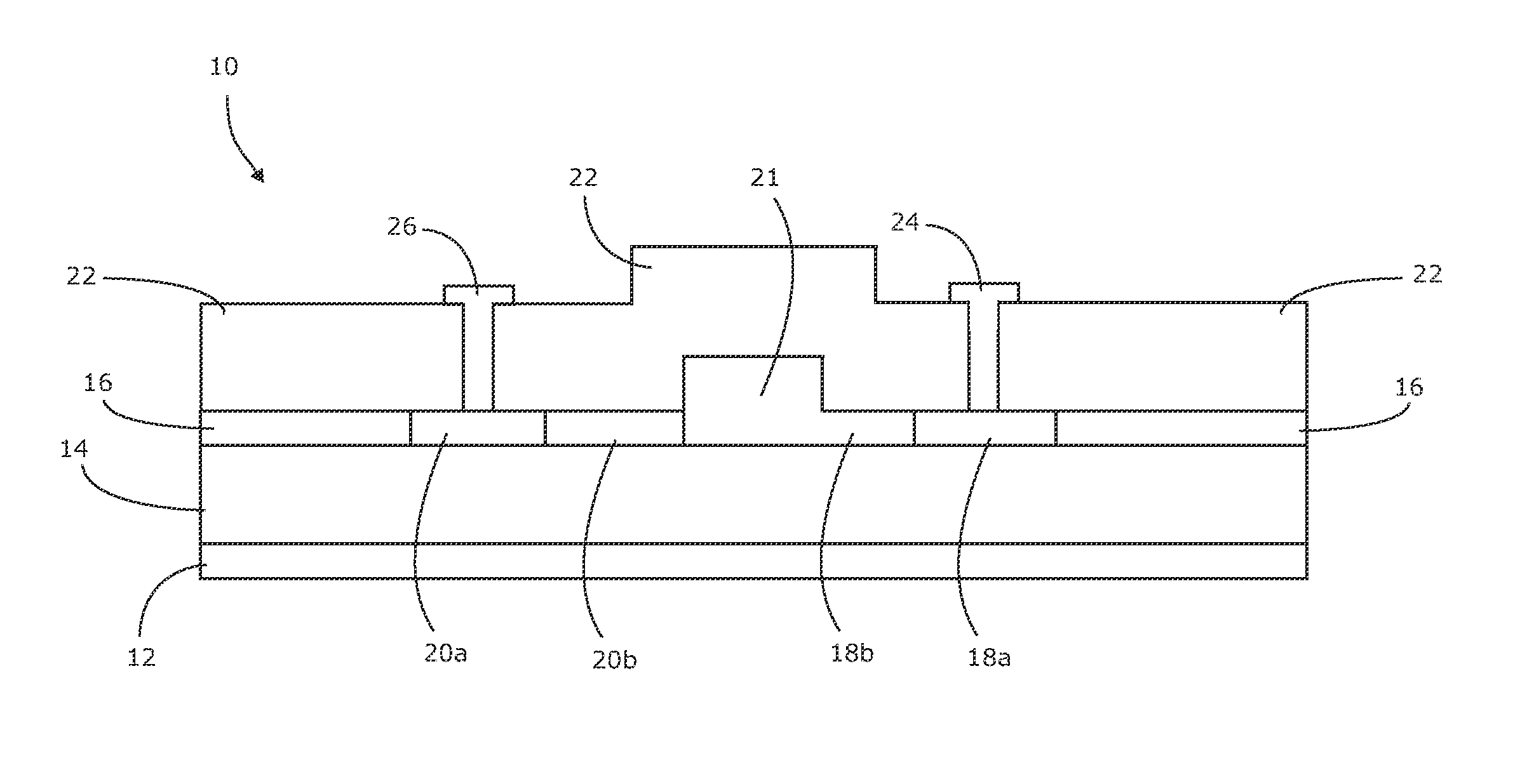
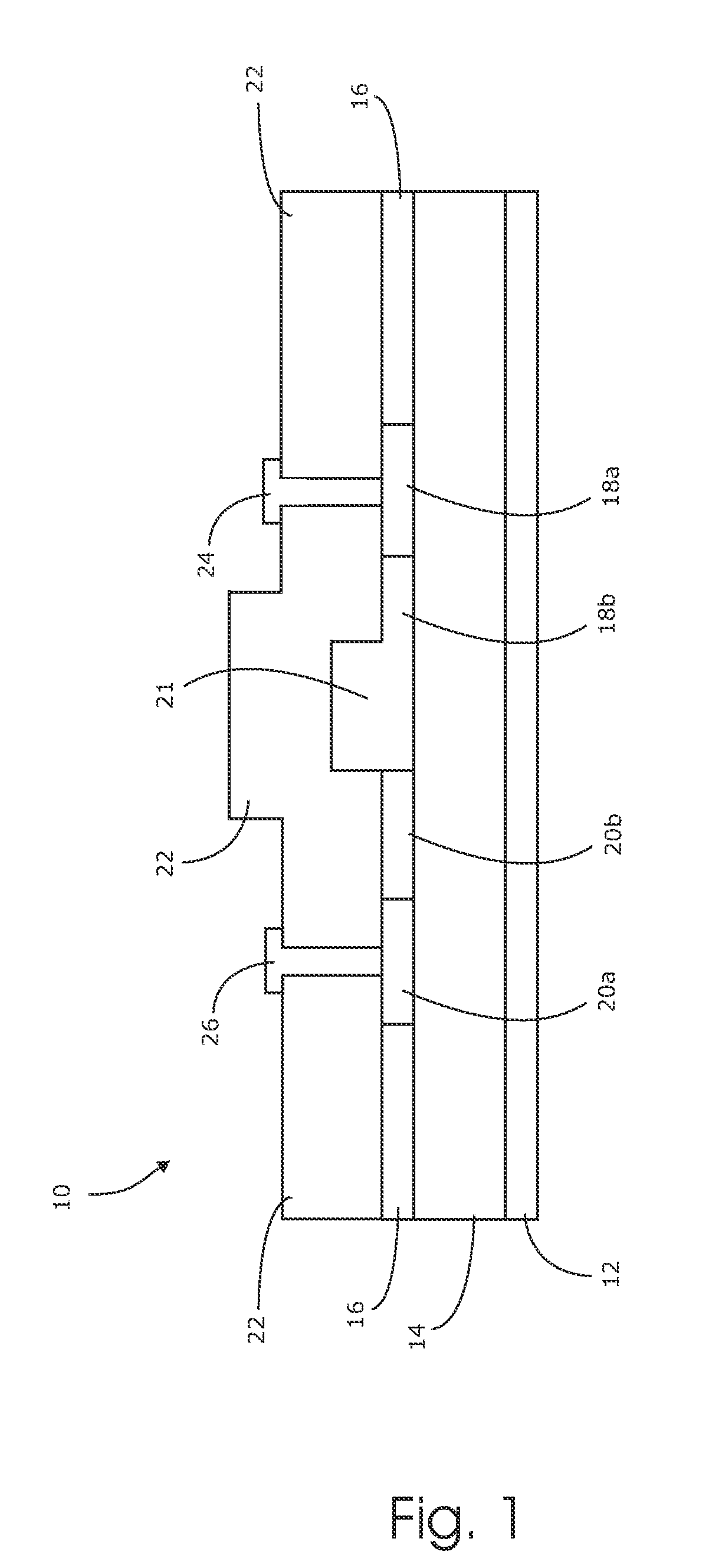
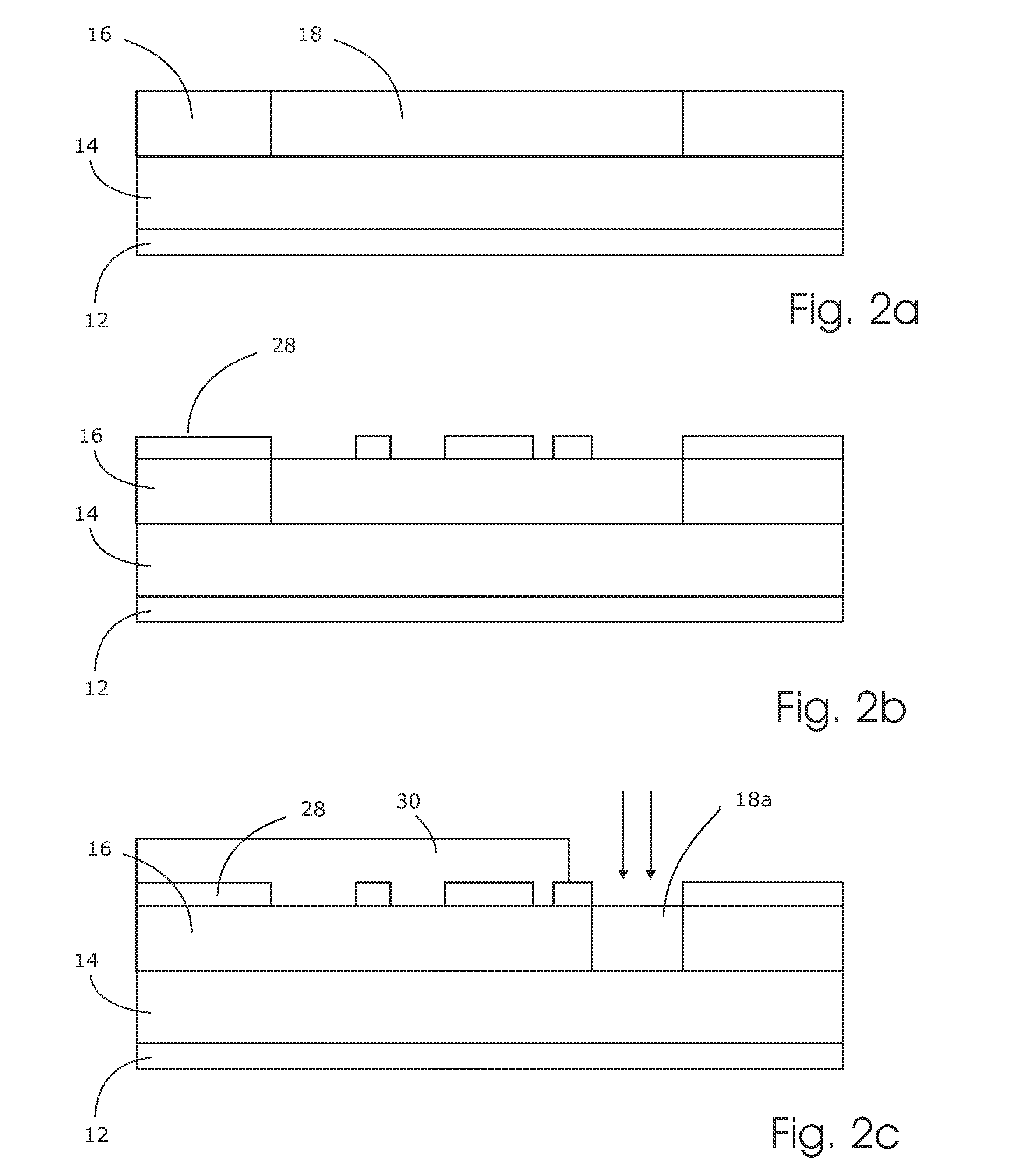
[0026]As stated above, conventional silicon electro-optic devices (such as electro-optic modulators) comprise a waveguide portion through which photons are transmitted. In operation, the free carrier concentration of the waveguide portion may be adjusted in order to change Its refractive index and control the passage of light through the device. This is usually achieved via a pn or pin junction, or MOS capacitor formed across / in the waveguide. However, the design of conventional devices has been such that their fabrication is difficult to achieve in CMOS processing.

[0027]According to embodiments of the present invention, an electro-optic device comprises a layer of light-carrying semiconductor material, such as silicon. The layer has two doped regions of opposite type, with one of the doped regions comprising a thicker waveguide rib through which photons are primarily conveyed. The other doped region abuts this waveguide rib, such that the pn junction so formed coincides with a side...


PUM


Abstract

An electro-optic device, comprising an insulating layer and a layer of light-carrying material adjacent the insulating layer. The layer of light-carrying material, such as silicon, comprises a first doped region of a first type and a second doped region of a second, different type abutting the first doped region to form a pn junction. The first doped region has a first thickness at the junction, and the second doped region has a second thickness at the junction, the first thickness being greater than the second thickness, defining a waveguide rib in the first doped region for propagating optical signals. Since the position of the junction coincides with the sidewall of the waveguide rib a self-aligned process can be used in order to simplify the fabrication process and increase yield.

Description

CROSS-REFERENCE TO RELATED APPLICATIONS[0001]The present application is the National stage application of PCT / GB2011 / 000060 filed Jan. 20, 2011 with the priority date of Jan. 22, 2010.FIELD OF THE INVENTION[0002]The present invention relates to the field of electro-optics, and particularly to electro-optic devices comprising a waveguide rib and methods for the fabrication thereof.BACKGROUND ART[0003]Silicon microphotonics has generated an increasing interest in recent years. Integrating optics and electronics on the same chip would allow enhancement of integrated circuit (IC) performance. Furthermore, telecommunications could benefit from the development of low cost solutions for high-speed optical links. The realization of active photonic devices, in particular high speed optical modulators integrated in silicon-on-insulator (SOI) waveguides, is essential for the development of silicon microphotonics / nanophotonics.[0004]Although silicon does not in normal circumstances exhibit a li...

Claims


Application Information

Patent Timeline
IPC IPC(8): G02B6/12H01L21/02
CPCG02F1/025G02B6/134G02F2201/063G02F2001/0152G02F1/0152H01L33/58G02B6/1347G02B6/136G02B2006/12173
Inventor THOMSON, DAVIDGARDES, FREDERICREED, GRAHAM
Owner POINTCLOUD INC
Why Eureka
Try Eureka