Power Module and Power Converter Containing Power Module

Active Publication Date: 2013-03-14
HITACHI ASTEMO LTD
View PDF1 Cites 62 Cited by
  • Summary
  • Abstract
  • Description
  • Claims
  • Application Information

AI Technical Summary

Benefits of technology

[0017]The present invention improves the reliability of the pow

Problems solved by technology

Attempting to pass a large electrical current flow through the power converter causes large heat emission from the semiconductor devices.
Unless the heat capacity of the power converter is gr

Method used


Image

  • Power Module and Power Converter Containing Power Module
  • Power Module and Power Converter Containing Power Module
  • Power Module and Power Converter Containing Power Module

Examples


Example

[0167]The above description of the first embodiment is now complete.

Example

[0168]The second embodiment is described next. The second embodiment utilizes a different shape for the auxiliary mold piece 600. In all other points the second embodiment is the same as the first embodiment.

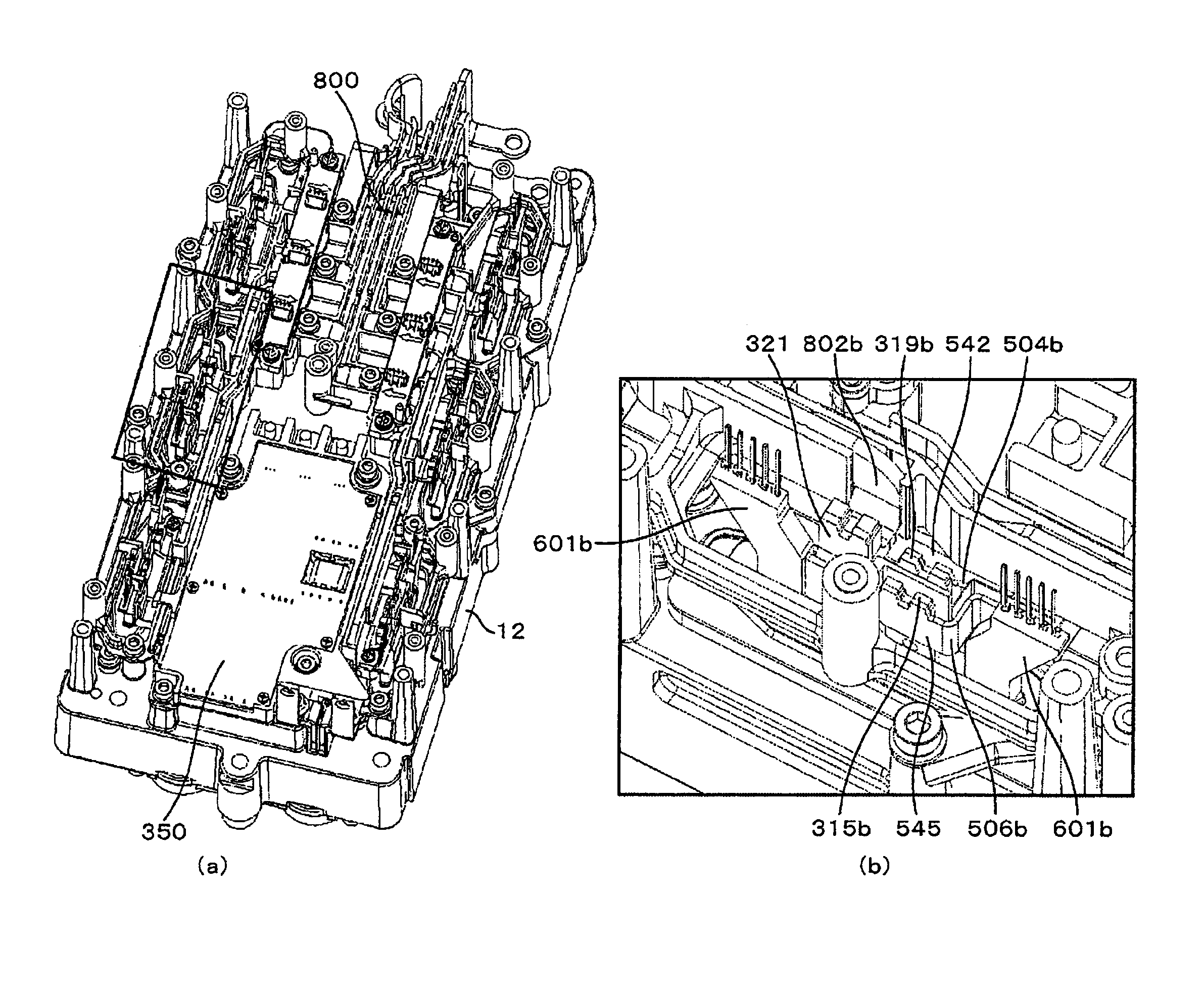
[0169](a) of FIG. 23 is a perspective view of the auxiliary mold piece 660 utilized in the second embodiment. (b) of FIG. 23 is a transparent view of the auxiliary mold piece 600.

[0170]The point here greatly differing from the first embodiment is that the DC positive terminal 315B and DC negative terminal 319B, and the AC terminal 321 are mounted between the external signal terminal 325U and external signal terminal 325L and supported in the auxiliary mold piece 660. This arrangement allows widening the welding space for the DC positive terminal 315B, DC positive terminal 319B, and the AC terminal 321 more than in the case when using the auxiliary mold piece 600 of the first embodiment. Widening the space for welding makes the signal conductor 324 less susceptible to effects fro...

Example

[0176]The third embodiment is described next while referring to FIG. 24.

[0177]The point here greatly differing from the first embodiment is that the DC negative wire 319A, the DC negative terminal 319B, and the fuse material 700 are not assembled into the single sheet shape in the first embodiment. The present embodiment newly utilizes an insert bus bar 711 where the DC negative wire 319A, the DC negative terminal 319B, and the fuse material 700 area single-sheet shape. In all other points the third embodiment is the same as the first embodiment.

[0178](a) of FIG. 24 is a view of the power module 300 without the module case 304 and the first sealer resin material 348. (b) of FIG. 24 is a view of the power module 300 in (a) of FIG. 24 installed in the module case 304. The fuse material 710 is adhered by caulking to the DC negative terminal 319B and the DC negative wire 319A. The first embodiment has the problem that the fuse material 700 is mounted away from the DC positive wire 315A ...


PUM


Abstract

A power module includes a semiconductor chip, a first coupling conductor with one main surface coupled to one main surface of the semiconductor chip, a second coupling conductor with one main surface coupled to the other main surface of the semiconductor chip, a coupling terminal supplied with electrical power from the direct current power source, and resin material to seal the semiconductor chip, and in which the resin member has a protruding section that protrudes from the space where the first and second coupling conductors are formed opposite each other, and the coupling terminal is clamped on the protruding section, and at least one of the first or second coupling conductors is coupled to a coupling terminal by way of a metallic material that melts at a specified temperature.

Description

TECHNICAL FIELD[0001]The present invention relates to a power module including internal semiconductor devices, and a power converter containing a power module.BACKGROUND ART[0002]In recent years, power converters must handle a large electrical current flow yet at the same meet demands for a small size. Attempting to pass a large electrical current flow through the power converter causes large heat emission from the semiconductor devices. Unless the heat capacity of the power converter is greatly improved, the semiconductor devices will reach a heat breakdown temperature due to their large heat emission but boosting the heat capacity prevents making the power converter smaller. Whereupon, a dual-sided cooling type power module was invented that improves the cooling efficiency by cooling the semiconductor element from both sides.[0003]In this dual-sided cooling type power module, lead frames serving as sheet conductors enclose both main surfaces of the semiconductor device; and a cool...

Claims


Application Information

Patent Timeline
IPC IPC(8): H01L27/04H01L23/48
CPCH01L2924/01012H01L2924/1305H01L25/18H02M1/32H02M7/003H05K7/1432H01L2924/0132H01L24/33H05K7/20927H01L2224/32245H01L2224/48227H01L2224/48472H01L2224/73265H01L2924/014H01L25/072H01L2924/1306H01L23/492H01L2924/3025H01L2924/30107H01L2924/3011H01L2924/13055H01L2224/48247H01L2224/48091H01L2924/01029H01L2224/291H01L2924/0133H01L2224/29111H01L2224/29109H01L2924/13091H01L2924/00H01L2924/0105H01L2924/01006H01L2924/01013H01L2924/01014H01L2924/0103H01L2924/01048H01L2924/01049H01L2924/01083H01L2924/00014H01L2924/351H01L2924/181H01L2224/33H01L2224/40137H01L24/40H01L2224/8484H01L2224/84801H01L2224/83801H01L2224/8384H05K7/14329H01L2924/00012H01L2224/73221
Inventor TOKUYAMA, TAKESHINAKATSU, KINYASATOH, TOSHIYAISHIKAWA, HIDEAKI
Owner HITACHI ASTEMO LTD
Why Eureka
Try Eureka