

Liquid crystal display apparatus
a technology of liquid crystal display and display device, which is applied in the direction of instruments, computing, electric digital data processing, etc., can solve the problems of deteriorating image quality, insufficient electric potential setting of the opposite electrode to the ground level, and inability to efficiently attract ions generated at a position away from the ion trap electrod
- Summary
- Abstract
- Description
- Claims
- Application Information
AI Technical Summary
Benefits of technology
Problems solved by technology
Method used
Image

Examples
embodiment 1
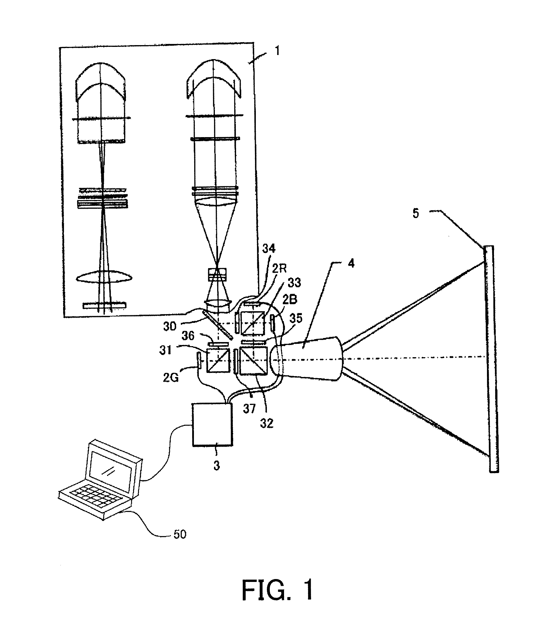
[0044]FIG. 1 shows the configuration of a liquid crystal projector (image projection apparatus) that is a first embodiment (Embodiment 1) of the present invention.
[0045]Reference numeral 3 denotes a liquid crystal driver serving as a controller. The liquid crystal driver 3 converts image information input from an image supply apparatus 50 such as a personal computer, a DVD player, and a television tuner into panel driving signals for red, green, and blue. The panel driving signals for red, green, and blue are respectively input to a liquid crystal panel 2R for red (R), a liquid crystal panel 2G for green (G), and a liquid crystal panel 2B for blue (B), all of which are reflective liquid crystal modulation elements. Thus, the three liquid crystal panels 2R, 2G, and 2B are individually controlled. The projector and the image supply apparatus 50 constitute an image display system.
[0046]The liquid crystal panels 2R, 2G, and 2B modulate light fluxes from an illumination optical system wh...
embodiment 2
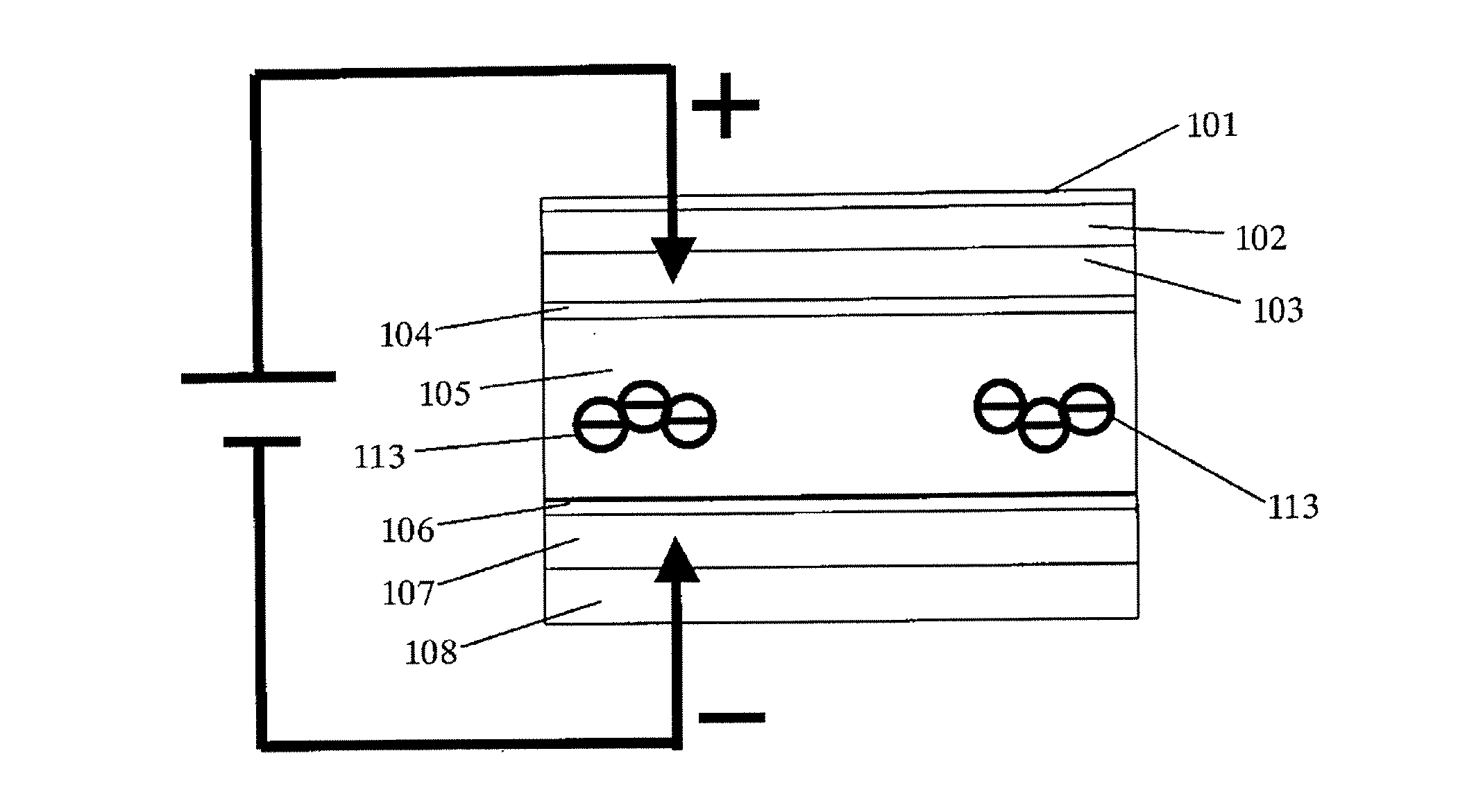
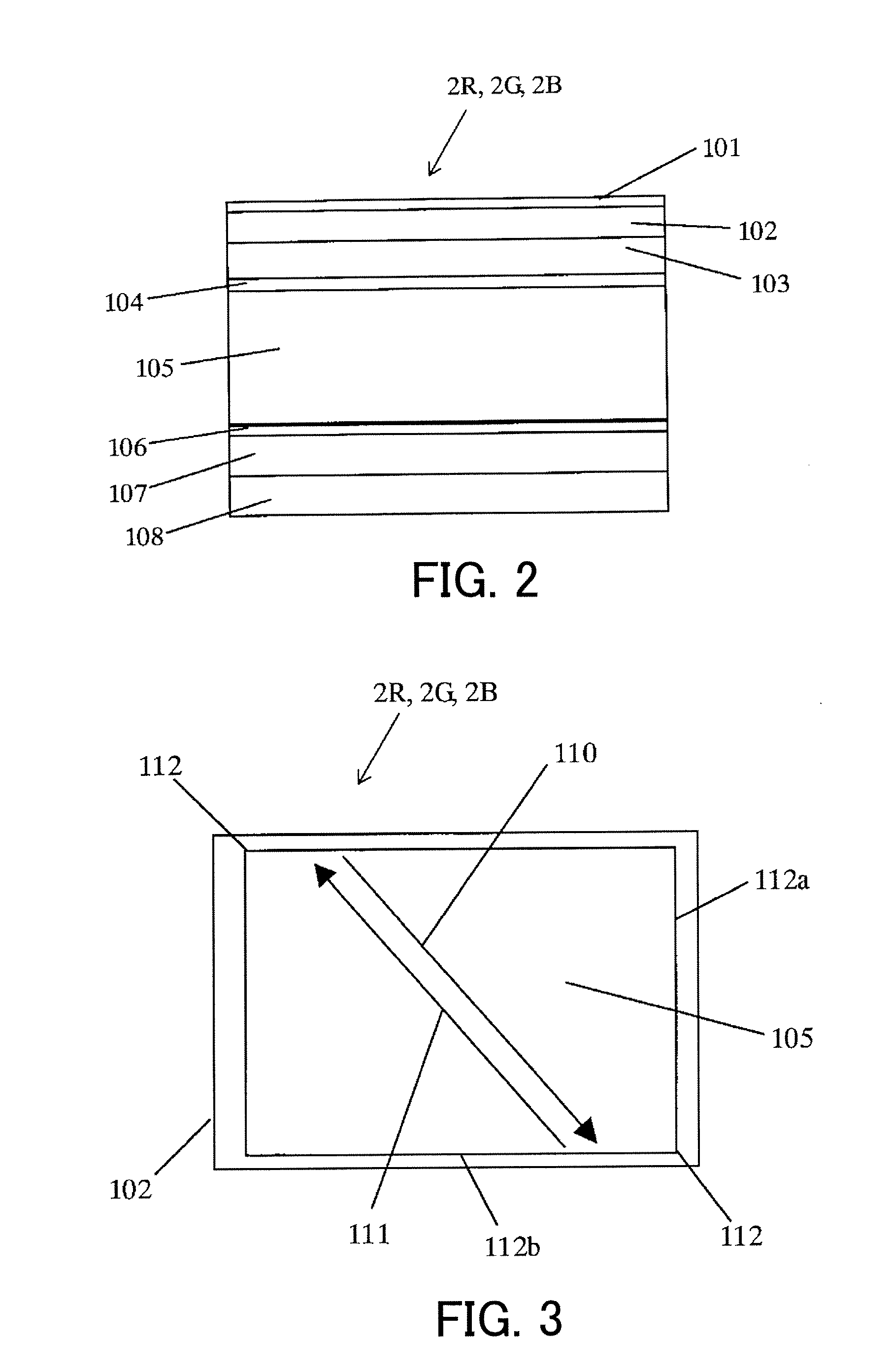
[0086]As described in Embodiment 1, the long-time use of the projector causes cumulation of the negative charged particles 113 in the vicinity of the diagonal areas which are areas in a diagonal direction of the effective display area 112 of the liquid crystal layer 105 on the side of the second alignment film 106.
[0087]In this second embodiment (Embodiment 2), the charged particles 113 are drawn in a direction different from the diagonal direction along which the charged particles 113 have accumulated, and thereby the accumulated charged particles 113 are diffused (or moved). Constituent elements in this embodiment common to those of Embodiment 1 are denoted with the same reference numerals. This is also applied to embodiments described later.
[0088]Also in this embodiment, in the modulation operation state, the voltages applied to the transparent electrode film 103 and the reflective pixel electrode layer 107 are controlled such that the alternating electric field described in FIG....
embodiment 3
[0106]As described in Embodiment 2, the long-time use of the projector causes the negative charged particles 113 to accumulate in the vicinity of the diagonal areas in one diagonal direction on the side of the second alignment film 106, the diagonal areas being in the effective display area 112 of the liquid crystal layer 105.
[0107]In this third embodiment (Embodiment 3), as in Embodiment 2, the charged particles 113 are drawn in a diagonal direction different from the diagonal direction along which the charged particles 113 have accumulated to diffuse them in the non-modulating operation state. Specifically, as described in Embodiment 2 with reference to FIG. 10, voltages are applied to the transparent electrode film 103 and the reflective pixel electrode layer 107 such that a difference between the voltages applied thereto (interelectrode electric potential difference) changes in the in-plane direction of the liquid crystal layer 105. More specifically, the voltages applied to the...
PUM
 Abstract
Description
Claims
Application Information