Interconnect board and electronic apparatus

a technology of interconnection board and electronic device, which is applied in the direction of cross-talk/noise/interference reduction, association of printed circuit non-printed electric components, cross-talk/noise/interference reduction, etc., can solve the problem of radiated noise that has propagated through the conductor, noise leakage outside other layers or multi-layer substrates, and inability to obtain sufficient noise countermeasures. to prevent the effect of noise radiation

Active Publication Date: 2013-03-21
NEC CORP
View PDF8 Cites 8 Cited by
  • Summary
  • Abstract
  • Description
  • Claims
  • Application Information

AI Technical Summary

Benefits of technology

[0009]The invention has been made in light of the above circumstances, and an object of the invention is to provide a interconnect board and an electronic apparatus which have a plurality of divided conductors and prevent leakage of noises irradiated from gaps between the conductors.
[0012]According to the invention, a interconnect board and an electronic apparatus which have a plurality of divided conductors and prevent leakage of noise radiated from gaps between the conductors are provided.

Problems solved by technology

In a case in which a plurality of conductors are formed on a conductor layer with gaps therebetween in an electronic apparatus having a multilayer substrate, when an electronic device is connected to the conductor, a noise that has propagated through the conductor is radiated from the gaps, and the noise leaks outside other layers or the multilayer substrate.
Therefore, it was not possible to obtain a sufficient noise countermeasure even when the EBG structure is configured in the conductor layer.

Method used


Image

  • Interconnect board and electronic apparatus
  • Interconnect board and electronic apparatus
  • Interconnect board and electronic apparatus

Examples


first embodiment

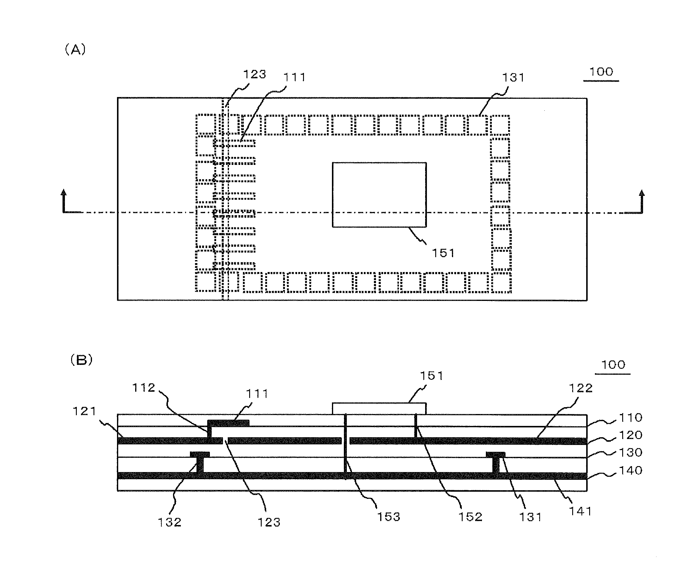
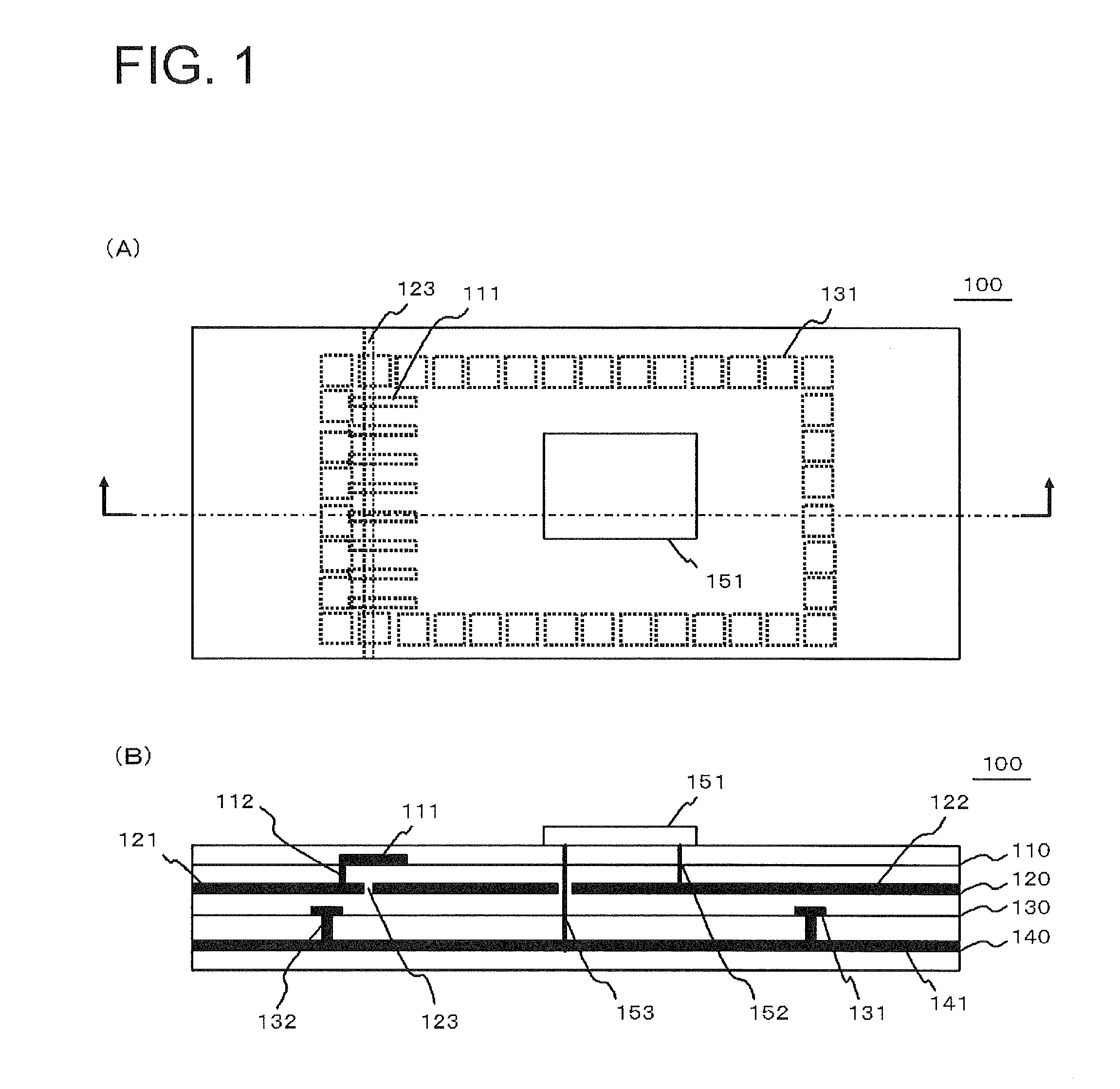
[0029]FIG. 1 shows a top view and a cross-sectional view of an electronic apparatus 100 according to a first embodiment of the invention. More specifically, FIG. 1A is a top view of the electronic apparatus 100, and FIG. 1B is a cross-sectional view of the electronic apparatus 100 at the cross-sectional line shown in FIG. 1A. The electronic apparatus 100 is a multilayer substrate having at least an A layer 110, a B layer 120, a C layer 130, and a D layer 140 sequentially from the top surface.

[0030]Meanwhile, the electronic apparatus 100 may have layers other than the above four layers. For example, the electronic apparatus may have dielectric layers located between the respective layers. In addition, the electronic apparatus 100 may further have holes or via holes, not shown, within the scope of the configuration of the invention. Furthermore, signal wires may be arrayed in the four layers within the scope of the configuration of the invention.

[0031]The electronic apparatus 100 has ...

second embodiment

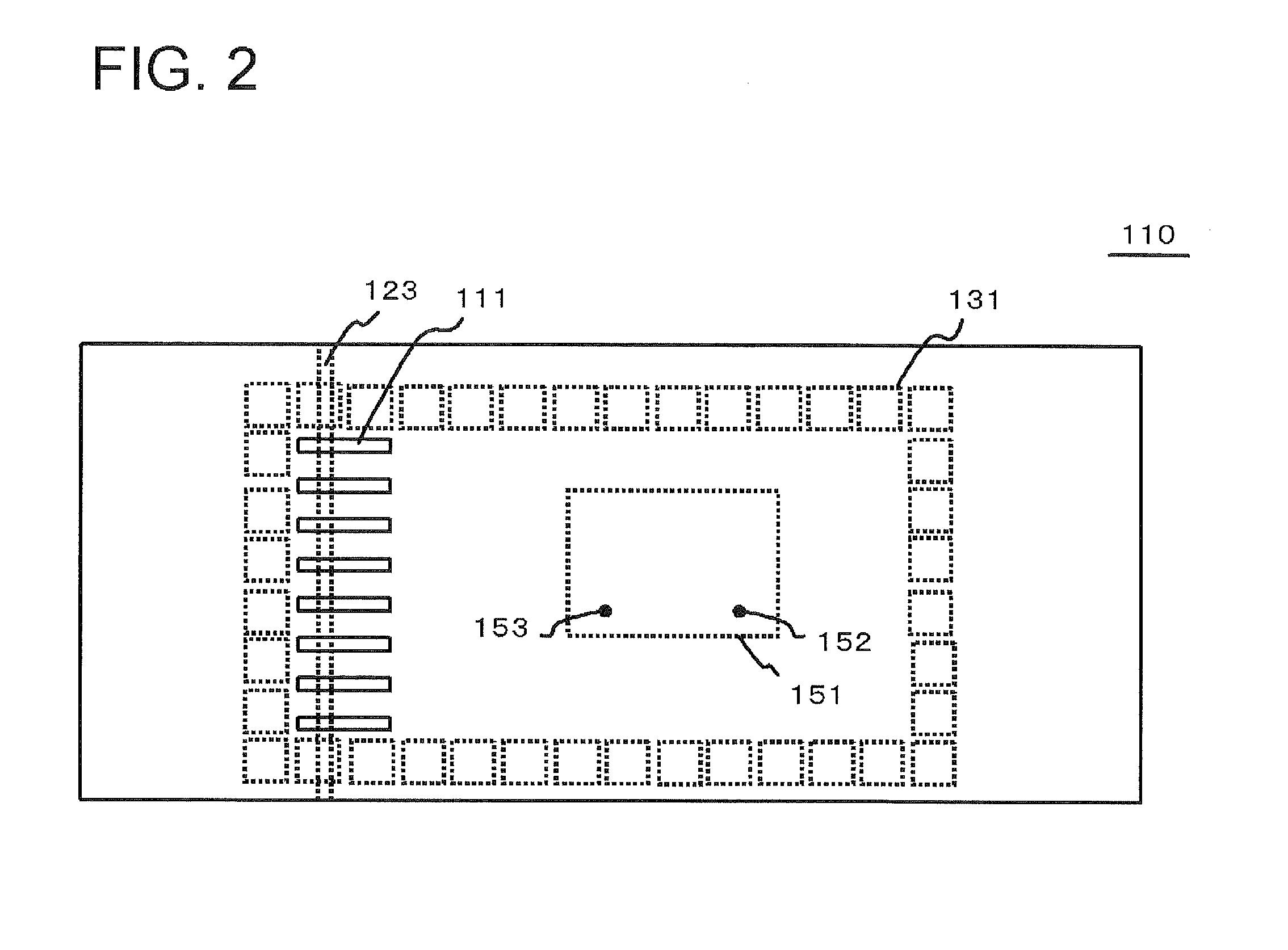
[0076]FIG. 7 shows a top view and a cross-sectional view of the electronic apparatus 100 according to a second embodiment of the invention. In more detail, FIG. 7A is a top view of the electronic apparatus 100, and FIG. 7B is a cross-sectional view of the electronic apparatus 100 at the cross-sectional line shown in FIG. 7A.

[0077]Compared to the electronic apparatus 100 of the first embodiment, the electronic apparatus 100 of the embodiment does not have the plurality of open stubs 111 and the A layer 110 on which the open stubs are located, and the difference is that, instead, a pectinate protrusion portion 124 is disposed at the gap 123 between the power supply plane 121 and the power supply plane 122. In other words, a plurality of recess portions are formed on a side facing the gap 123 in the power supply plane 122, and the protrusion portion 124 integrally formed with the power supply plane 121 is inserted into the respective plurality of recess portions.

[0078]FIG. 8 is a view ...


PUM


Abstract

An electronic apparatus (100) has an electronic device (151), a power supply plane (121) and a power supply plane (122) disposed with a gap (123) therebetween, a connection member (152) that electrically connects the power supply plane (122) and the electronic device (151), a ground plane (141) facing the power supply plane (121) or the power supply plane (122), a connection member (153) that electrically connects the ground plane (141) and the electronic device (151), a plurality of conductor elements (131) that is repeatedly arrayed, and open stubs (111) formed at a location overlapping the gap (123) included in an area surrounded by the conductor elements (131). In addition, at least some of the open stubs (111) face the power supply plane (122) which is not in contact with the open stubs (111).

Description

TECHNICAL FIELD[0001]The present invention relates to a interconnect board and an electronic apparatus.BACKGROUND ART[0002]In an electronic apparatus, there are cases in which noise generated from electronic devices propagates through a parallel plate including a power supply and a ground plane that serves as a kind of waveguide so as to adversely affect other electronic devices or adjacent wireless circuits and the like. Therefore, in electronic apparatuses, it is normal to implement noise countermeasures, and a number of techniques have been developed.[0003]In recent years, it has become evident that the propagation characteristics of electromagnetic waves can be controlled by disposing conductor patterns having a specific structure periodically (hereinafter described as a metamaterial). Particularly, a metamaterial configured to control electromagnetic wave propagation in a specific frequency zone is referred to as an electromagnetic band gap structure (hereinafter described as a...

Claims


Application Information

Patent Timeline
Patent Type & Authority Applications(United States)
IPC IPC(8): H05K1/18H05K1/11
CPCH05K1/0236H05K1/0224
Inventor TOYAO, HIROSHIKUSUMOTO, MANABUKOBAYASHI, NAOKIANDO, NORIAKI
Owner NEC CORP
Why Eureka
Try Eureka