

Manufacturing method for display device having a plurality of thin film transistors and display device formed thereby
a manufacturing method and thin film transistor technology, applied in the direction of semiconductor devices, electrical appliances, basic electric elements, etc., can solve the problems of contaminated thin film transistors, negative influence on the operation of thin film transistors, and low productivity of used photoresist masks, so as to improve productivity and improve quality. , the effect of good quality images
- Summary
- Abstract
- Description
- Claims
- Application Information
AI Technical Summary
Benefits of technology
Problems solved by technology
Method used
Image

Examples
Embodiment Construction
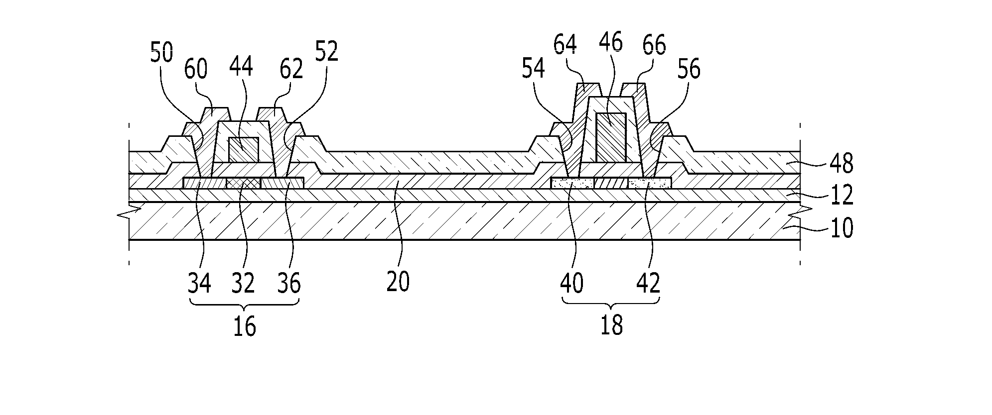
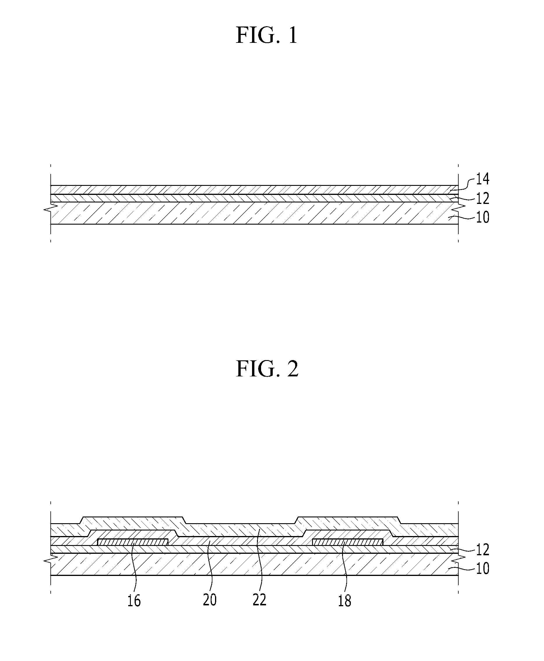
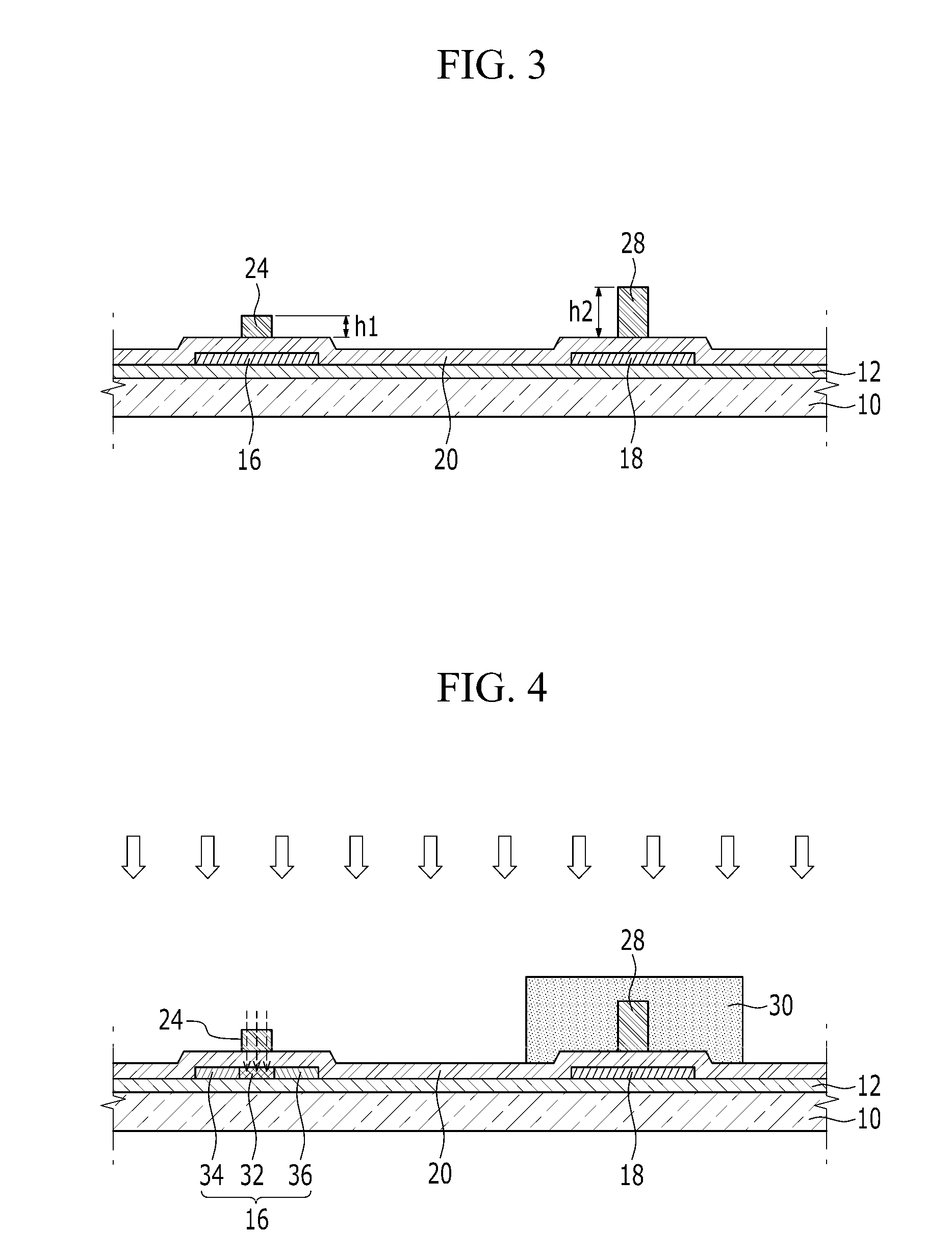
[0026]The present invention will be described more fully hereinafter with reference to the accompanying drawings, in which embodiments of the invention are shown. As those skilled in the art would realize, the described embodiments may be modified in various different ways, all without departing from the spirit or scope of the present invention.
[0027]In order to elucidate the present invention, parts that are not related to the description may be omitted. Like reference numerals designate like elements throughout the specification.
[0028]In addition, the size and thickness of each component shown in the drawings are arbitrarily shown for ease of understanding and description, but the present invention is not limited thereto.
[0029]In the drawings, the thickness of layers, films, panels, regions, etc., are exaggerated for clarity. In addition, in the drawings, for understanding and ease of description, the thicknesses of some layers and areas are exaggerated. It will be understood that...
PUM
 Abstract
Description
Claims
Application Information