Plasma processing apparatus

a plasma processing and plasma technology, applied in the field of plasma processing equipment, can solve the problems of reducing the production yield of devices, difficult to make a plasma of a uniform density in the processing space of the chamber, and difficult to flatten the plasma density distribution, so as to improve the in-plane uniformity of the plasma density and the plasma process, and widen the rf power rang

Active Publication Date: 2013-03-28
TOKYO ELECTRON LTD
View PDF5 Cites 4 Cited by
  • Summary
  • Abstract
  • Description
  • Claims
  • Application Information

AI Technical Summary

Benefits of technology

[0010]In view of the above, the present invention provides a plasma processing apparatus capable of improving in-plane uniformity of a plasma process in wide RF frequency and power ranges.
[0013]In this configuration, when the RF power from the RF power supply unit goes around into the electrode main surface (top surface) along a surface layer of the lower electrode, a part of the RF power is emitted out of the periphery portion of the top surface of the electrode. Since the RF ground member receives the part of the RF power and sends it to the ground line, the part of the RF power makes no contribution to discharge of the processing gas, i.e., plasma generation. Thus, a plasma generation region in the processing space is confined to a region right above or near the substrate to be processed and a profile of the plasma density distribution on the substrate can be stabilized.
[0016]In this configuration, when the RF power from the RF power supply unit goes around into the electrode main surface (top surface) along a surface layer of the lower electrode, a part of the RF power is emitted out of the periphery portion of the top surface and a side surface of the electrode. Since the RF ground member receives the part of the RF power and sends it to the ground line, the part of the RF power makes no contribution to discharge of the processing gas, i.e., plasma generation. Thus, a plasma generation region in the processing space is confined to a region right above or near the substrate to be processed and a profile of the plasma density distribution on the substrate can be stabilized. In addition, the RF ground member may preferably covers a substantially entire region of the top surface of the lower electrode projecting outwardly in radial directions from the substrate.
[0018]It is preferable that an annular gas exhaust path for connecting the processing space to a gas exhaust port provided at a bottom portion of the processing chamber may be formed between the RF ground member and an inner wall of the processing chamber, and a plurality of conductive fin members, which is electrically grounded and vertically extending, for promotion of extinction of a plasma diffused from the processing space is provided at an upper region of the gas exhaust path. This plasma extinction promotion function of the fin members may reduce plasma existing near or above the entrance of the gas exhaust path, thereby relatively increasing the plasma density of a region right above the wafer while reducing altitude differences in the plasma density distribution.
[0021]The RF power may have a frequency equal to or higher than 80 MHz. With such configuration, it is possible to improve in-plane uniformity of a plasma density and a plasma process in wide RF power ranges. Further, another RF power is applied to the lower electrode to attract ions in the plasma mainly towards the substrate disposed on the lower electrode from another RF power supply unit.
[0022]In accordance with the plasma processing apparatus of the present invention with the above-described configuration and operation, it is possible to improve in-plane uniformity of a plasma process in wide RF frequency and power ranges.

Problems solved by technology

Here, it becomes difficult to make a plasma of a uniform density in a processing space of the chamber (particularly in a radial direction).
If the plasma density is non-uniform above the substrate, a plasma process also becomes non-uniform, which leads to a reduced production yield of devices.
However, if a frequency of the employed RF power is increased further, variation of the plasma density distribution (altitude difference in the mountain-like distribution) becomes larger in proportion to the increased frequency, thereby making it difficult to flattening the plasma density distribution.
In addition, a cathode-coupled plasma processing apparatus is disadvantageous in that, if a frequency of the RF power exceeds about 80 MHz, a plasma density distribution produced by an RF power of a certain power level becomes to have a W-like profile in which the plasma density is high above the central portion and the edge portion of a substrate and low above the portion therebetween.

Method used


Image

  • Plasma processing apparatus
  • Plasma processing apparatus
  • Plasma processing apparatus

Examples


Embodiment Construction

[0034]Hereinafter, embodiments of the present invention will be described with reference to the accompanying drawings which form a part hereof

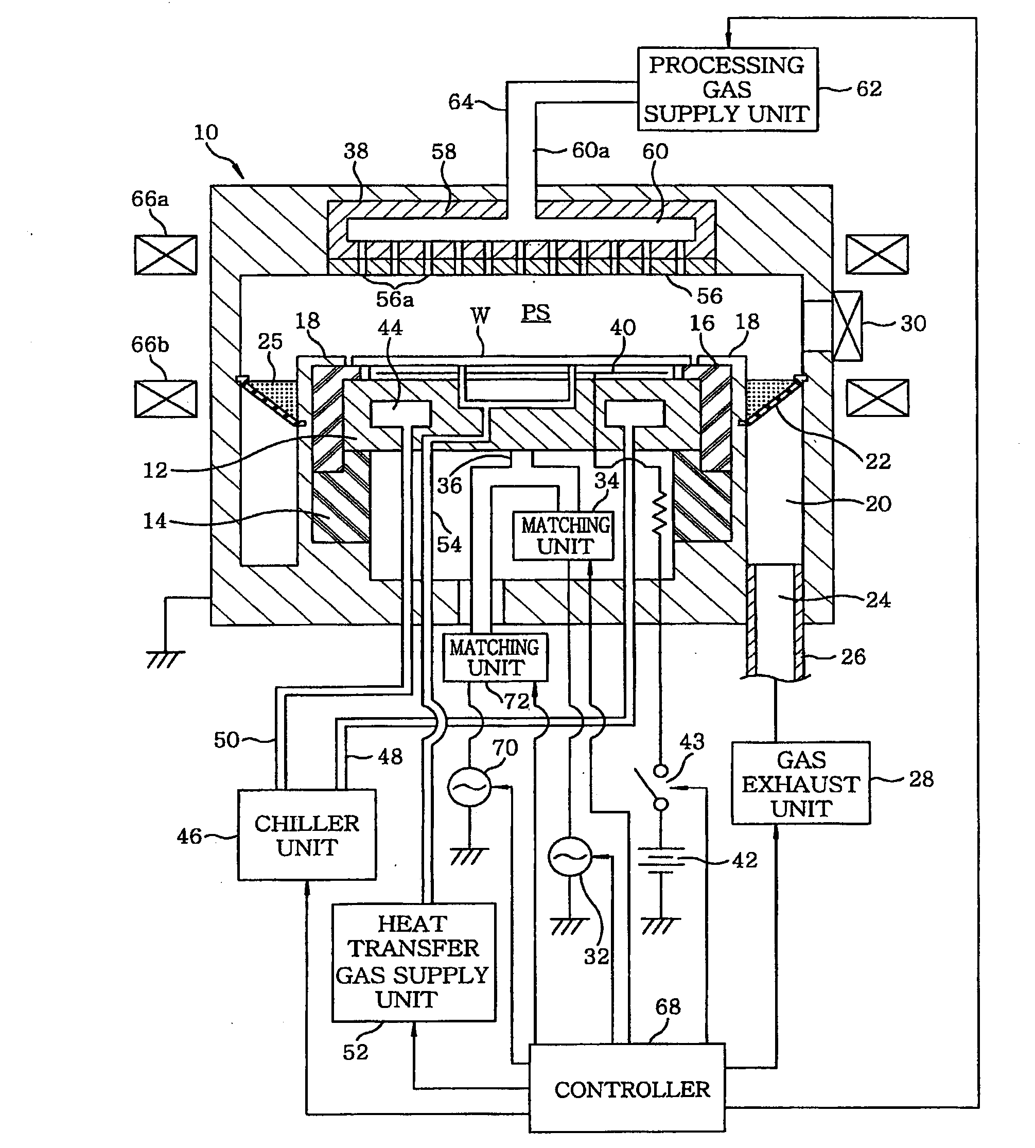
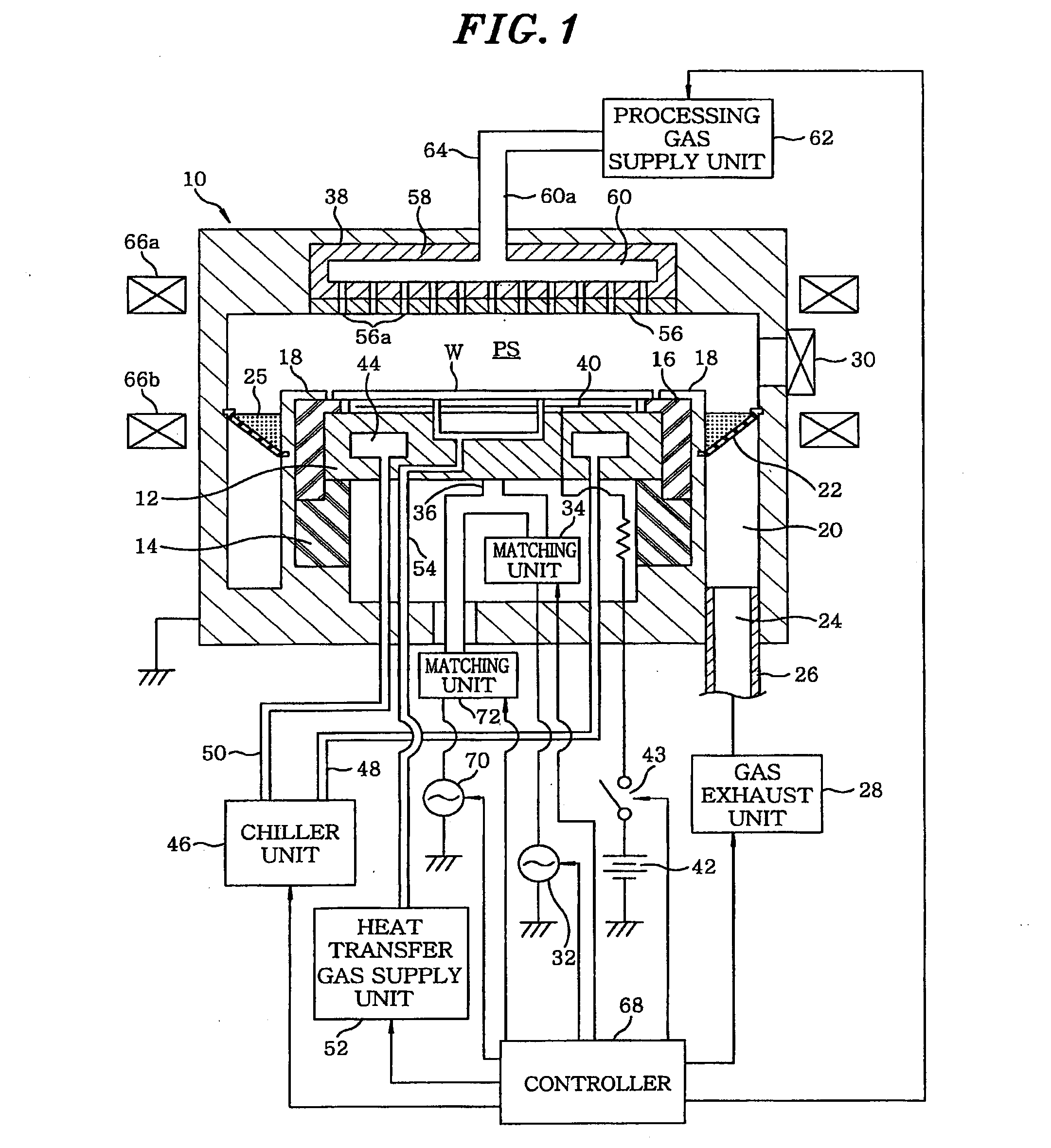
[0035]FIG. 1 shows a configuration of a plasma etching apparatus in accordance with an embodiment of the present invention. The plasma processing apparatus is configured as a capacitively coupled plasma etching apparatus of a cathode coupling type (lower electrode dual frequency application type) in which dual radio frequency (RF) powers are applied to a lower electrode, and includes a cylindrical chamber (processing chamber) 10 made of metal such as aluminum, stainless steel or the like. The chamber 10 is frame grounded.

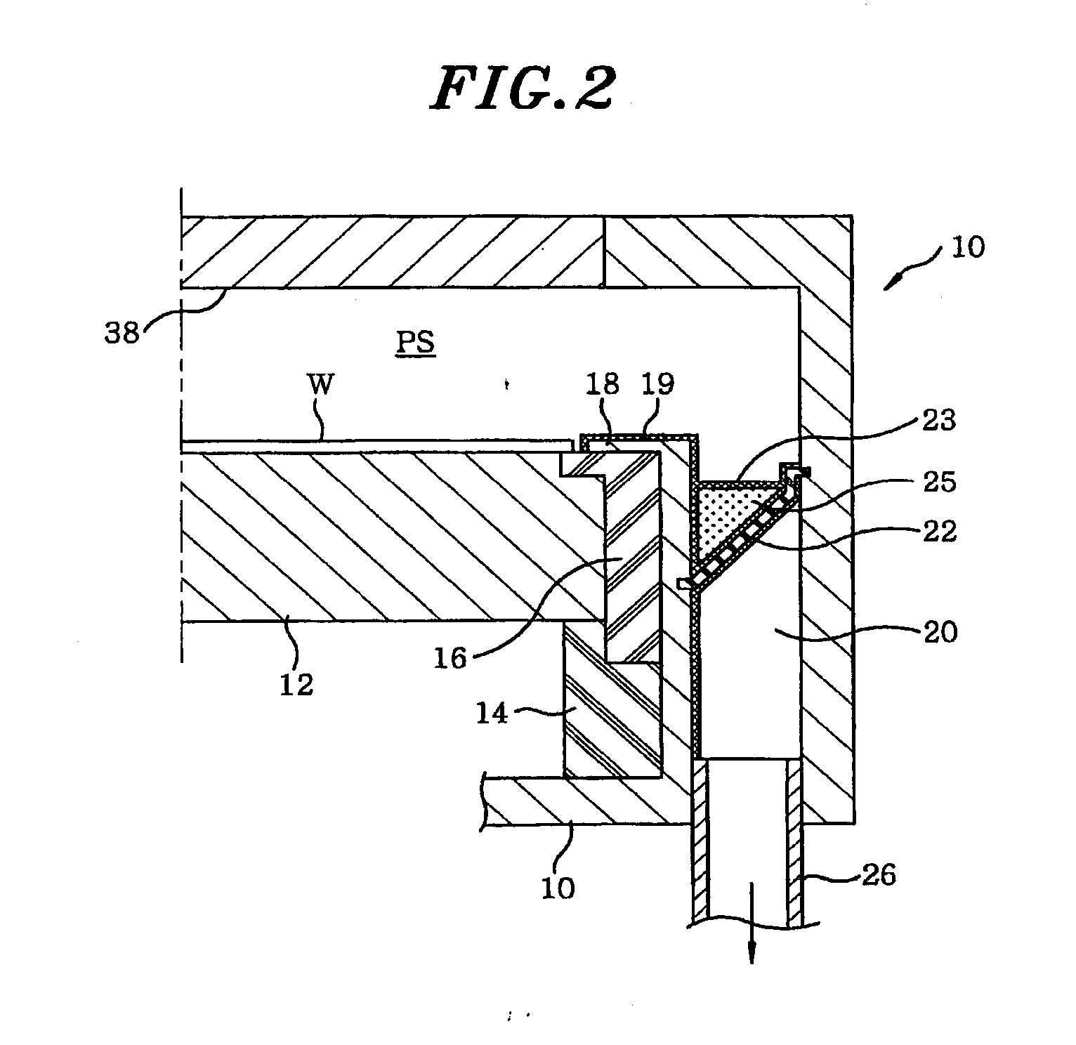
[0036]A circular plate-shaped lower electrode or a susceptor 12 for mounting thereon a substrate to be processed, e.g., a semiconductor wafer W, is installed in the chamber 10. The susceptor 12 is made of a conductive material, e.g., aluminum, and is supported by the bottom wall of the chamber 10 through a cylindrical support ...


PUM

PropertyMeasurementUnit
frequencyaaaaaaaaaa
frequencyaaaaaaaaaa
frequencyaaaaaaaaaa

Abstract

A plasma processing apparatus includes a processing gas supplying unit for supplying a desired processing gas to a processing space between an upper electrode and a lower electrode which are disposed facing each other in an evacuable processing chamber. The plasma processing apparatus further includes a radio frequency (RF) power supply unit for applying an RF power to one of the lower and the upper electrode to generate plasma of the processing gas by RF discharge and an electrically conductive RF ground member which covers a peripheral portion of the electrode to which the RF power is applied to receive RF power emitted outwardly in radial directions from the periphery portion of the electrode to which the RF power is applied and send the received RF power to a ground line.

Description

CROSS-REFERENCE TO RELATED APPLICATIONS[0001]This application is a division of and claims the benefit of priority from U.S. Ser. No. 12 / 407,922, filed Mar. 20, 2009, and the present application further claims the benefit of priority of U.S. Ser. No. 61 / 092,626, filed Aug. 28, 2008, and further the present application is based upon and claims the benefit of priority from the prior Japanese Patent Application No. 2008-073376, filed Mar. 21, 2008; the entire content of each of the foregoing is incorporated herein by reference.FIELD OF THE INVENTION[0002]The present invention relates to a technique for performing a plasma processing on a substrate to be processed, and more particularly, to a capacitively coupled plasma processing apparatus.BACKGROUND OF THE INVENTION[0003]In a manufacturing process of a semiconductor device or an FPD (flat panel display), a plasma is often used in the process, e.g., etching, deposition, oxidation, sputtering or the like, in order to allow a processing g...

Claims


Application Information

Patent Timeline
Patent Type & Authority Applications(United States)
IPC IPC(8): H01L21/3065
CPCH01J37/32091H01L21/3065H01J37/32642H01J37/32577H01L21/205
Inventor MATSUDO, TATSUOHIMORI, SHINJI
Owner TOKYO ELECTRON LTD
Why Eureka
Try Eureka