Semiconductor device

a technology of semiconductor devices and semiconductors, applied in semiconductor devices, semiconductor/solid-state device details, electrical apparatus, etc., can solve the problems of increasing the amount of segregated au, reducing joint strength, and causing bump cracks, etc., and achieve the effect of suppressing thin-filming

Inactive Publication Date: 2013-04-04
PS4 LUXCO SARL
View PDF2 Cites 15 Cited by
  • Summary
  • Abstract
  • Description
  • Claims
  • Application Information

AI Technical Summary

Benefits of technology

[0027]In the present invention, sub-bumps greater in height than main bumps are provided, so that the sub-bumps come into contact with one another earlier than the main bumps and serve as stoppers at the time of joining the main bumps. Consequently, it is possible to suppress the thin-filming of a layer between joined main bumps, such as a solder layer, to be fluidized by heating, and therefore, provide a high-reliability semiconductor device.

Problems solved by technology

This may decrease joint strength and induce bump cracks.
The amount of segregated Au increases in particular and cracks occur if thermal stress caused by a reliability test or the like is applied.
In addition, a previous solder reflow process may not be fully carried out in some cases for reasons of process steps.

Method used


Image

  • Semiconductor device
  • Semiconductor device
  • Semiconductor device

Examples


exemplary embodiment 1

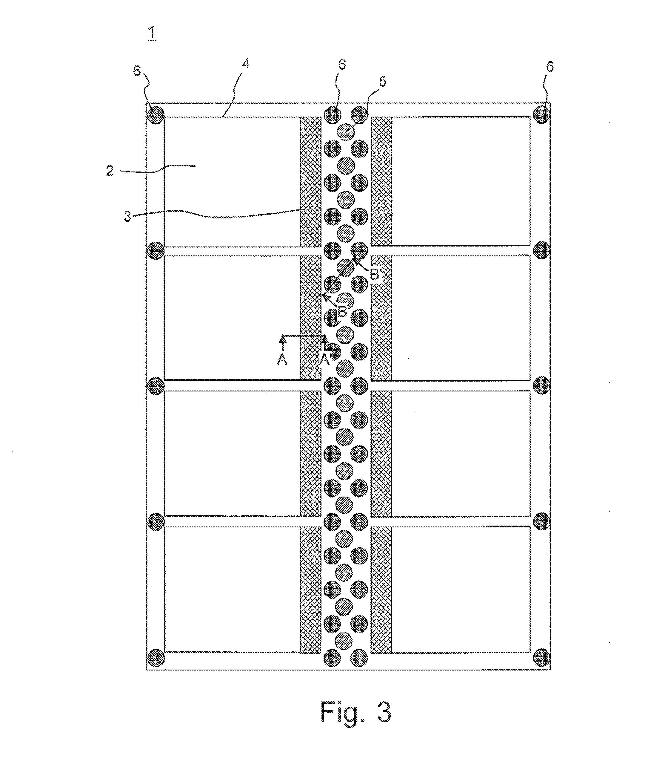
[0050]FIGS. 4A and 5A are cross-sectional process drawings, as viewed along the A-A′ line of FIG. 3, used to describe a process of manufacturing a semiconductor chip according to Exemplary Embodiment 1 of the present invention, whereas FIGS. 4B, 5B, 6 to 13, 14A, 14B, 15 to 18, and 20 are cross-sectional process drawings which are used to describe the process of manufacturing the semiconductor chip according to Exemplary Embodiment 1 and correspond to cross-sectional views taken along the B-B′ line of FIG. 3. Note that a scale in each figure is optional and differs from the scale of an actual device configuration.

[0051]First, as illustrated in FIG. 4A, STIs 12 for element isolation are formed in memory cell region 2 and peripheral circuit region 3 of semiconductor substrate 7. On the other hand, as illustrated in FIG. 4B, annular insulating region 11 for ensuring insulation from a semiconductor element and the like, which are formed in memory cell region 2 and peripheral circuit reg...

exemplary embodiment 2

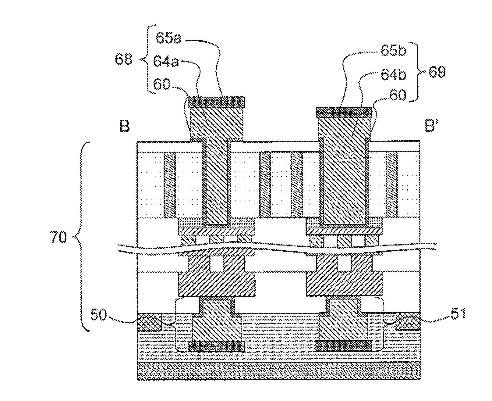
[0073]In the formation of a front bump in Exemplary Embodiment 1, offsets D1 of 30 μm are secured for both first sub-bump hole 40 and first main bump hole 41 to form PIQ hole pattern 43, so that the first sub-bump and the first main bump are the same in shape. In the present exemplary embodiment, however, PIQ hole pattern 43a surrounding first sub-bump hole 40 is formed so that the diameter of the hole pattern is the same as or larger, within the upper limit of approximately 2 μm, than diameter D0 of first sub-bump hole 40. On the other hand, PIQ hole pattern 43b surrounding first main bump hole 41 is formed while securing offset D1 of 30 μm as in Exemplary Embodiment 1 (FIG. 22).

[0074]Next, photoresist 45 is formed after first feed layer 44 is formed in the same way as in Exemplary Embodiment 1. Then, first sub-bump opening pattern 46 and first main bump opening pattern 47 having diameter D3 are likewise formed. Thereafter, Cu film 48 is grown by a plating method (FIG. 23).

[0075]Si...

exemplary embodiment 3

[0079]In the steps of FIGS. 15 and 16 in Exemplary Embodiment 1, second sub-bump hole 58 is formed so as to be smaller in diameter (D4) than second main bump hole 59, in the present exemplary embodiment, however, an example is shown in which after second sub-bump hole 58 is formed so as to be the same in diameter (D5) as second main bump hole 59, the diameters of openings formed in a photoresist to serve as a plating mask are varied to make a height variation between second sub-bump hole 58 and second main bump hole 59.

[0080]First, rear-surface protective film 54 is formed after carrying out steps up to the step of FIG. 14 in the same way as in Exemplary Embodiment 1. Then, second sub-bump hole pattern 56 and second main bump hole pattern 57 are formed in photoresist 55, so as to have diameter D5, and etching is performed in the same way as in Exemplary Embodiment 1. This process forms second sub-bump hole 58w and second main bump hole 59 having diameter D5, as illustrated in FIG. 2...


PUM


Abstract

First and second sub-bumps are provided on both surfaces of each substrate along with a usual bump structure (first and second main bumps), and at least one of the first and second sub-bumps is made greater in height than the first and second main bumps, so that the sub-bumps come into contact with one another earlier than the main bumps at the time of joining semiconductor chips, thereby securing margins of joint among the main bumps and suppressing the thin-filming of a layer, such as a solder layer, to be fluidized by heating.

Description

BACKGROUND OF THE INVENTION[0001]1. Field of the Invention[0002]The present invention relates to a semiconductor device, and more particularly, to a semiconductor device provided with an electrode penetrating through a substrate.[0003]2. Description of the Related Art[0004]Along with the functional upgrading and the diversification of semiconductor devices, there has recently been proposed a semiconductor device integrated by vertically stacking a plurality of semiconductor chips. Such a semiconductor device is configured to achieve electrical conduction between respective semiconductor chips by an electrode penetrating through the substrate of each semiconductor chip. The electrode penetrating through the substrate is so-called a through silicon via (TSV).[0005]For example, JP2010-272737A discloses a method of connecting a plurality of semiconductor chips including TSVs. Bumps are formed on each TSV as connecting terminals on both sides of a semiconductor chip. The bumps include a ...

Claims


Application Information

Patent Timeline
Patent Type & Authority Applications(United States)
IPC IPC(8): H01L23/485H01L25/03
CPCH01L2224/16225H01L2924/15311H01L2924/00014H01L2225/06541H01L2225/06513H01L25/50H01L25/0657H01L23/481H01L2224/13111H01L2224/17055H01L2224/05572H01L2224/11002H01L2224/81815H01L2224/81203H01L2224/81193H01L2224/16146H01L2224/14181H01L2224/1403H01L2224/13155H01L2224/13147H01L2224/13144H01L2224/13083H01L2224/05027H01L21/76898H01L24/03H01L24/05H01L24/06H01L24/11H01L24/13H01L24/14H01L24/16H01L24/17H01L21/6836H01L24/81H01L2221/68327H01L2221/6834H01L2224/0401H01L2224/05166H01L2224/05647H01L2224/06102H01L2224/11462H01L2224/1147H01L2224/13009H01L2924/00012H01L2924/01047H01L2224/05552H01L2924/351H01L2924/15788H01L2224/141H01L2924/00
Inventor TORII, KOJI
Owner PS4 LUXCO SARL
Why Eureka
Try Eureka