Fast-settling precision voltage follower circuit and method
a follower circuit and precision technology, applied in the direction of electric variable regulation, process and machine control, instruments, etc., can solve the problem of not providing the short settling time required for a capacitive touch screen application
- Summary
- Abstract
- Description
- Claims
- Application Information
AI Technical Summary
Benefits of technology
Problems solved by technology
Method used
Image
Examples
Embodiment Construction
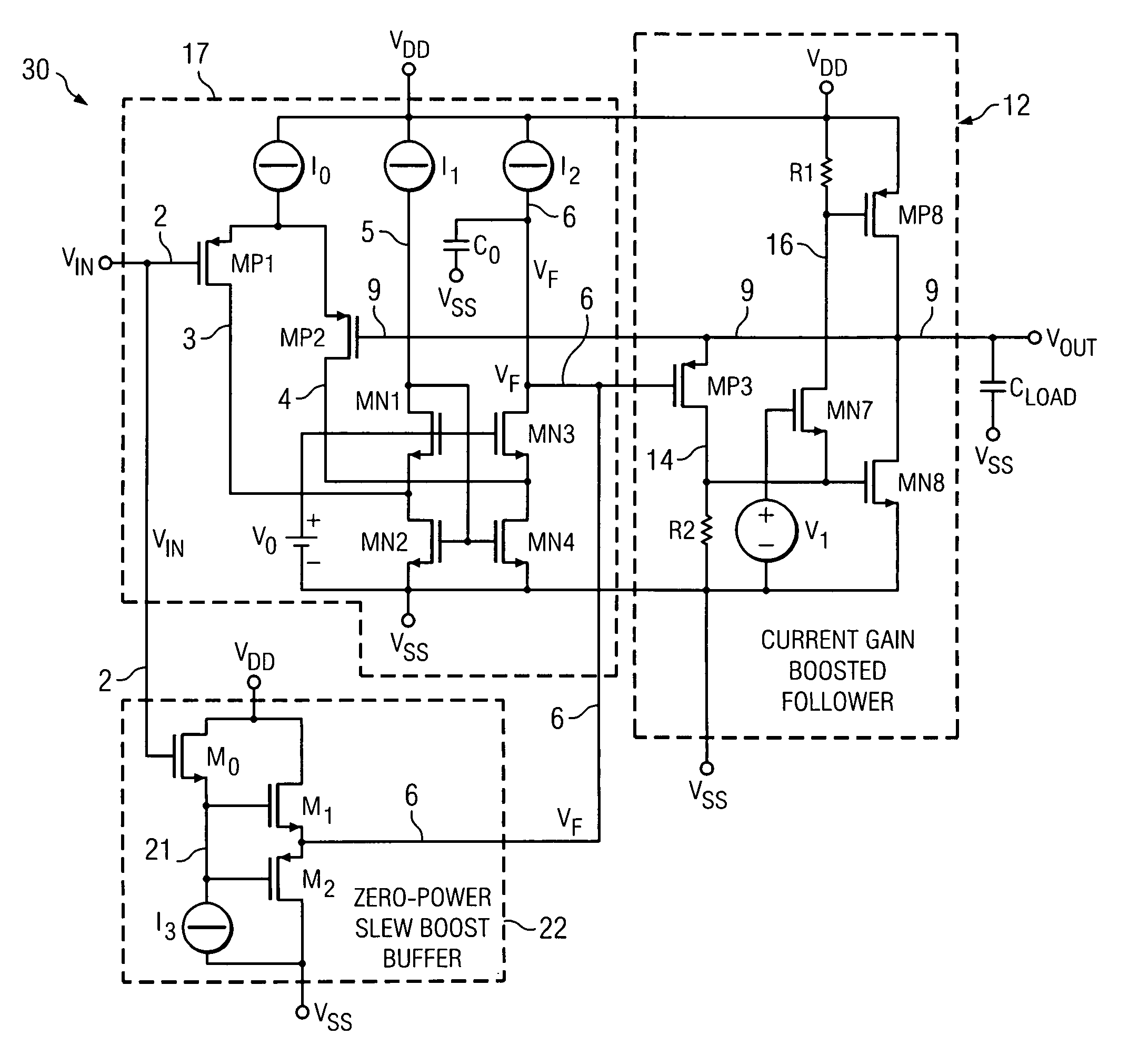
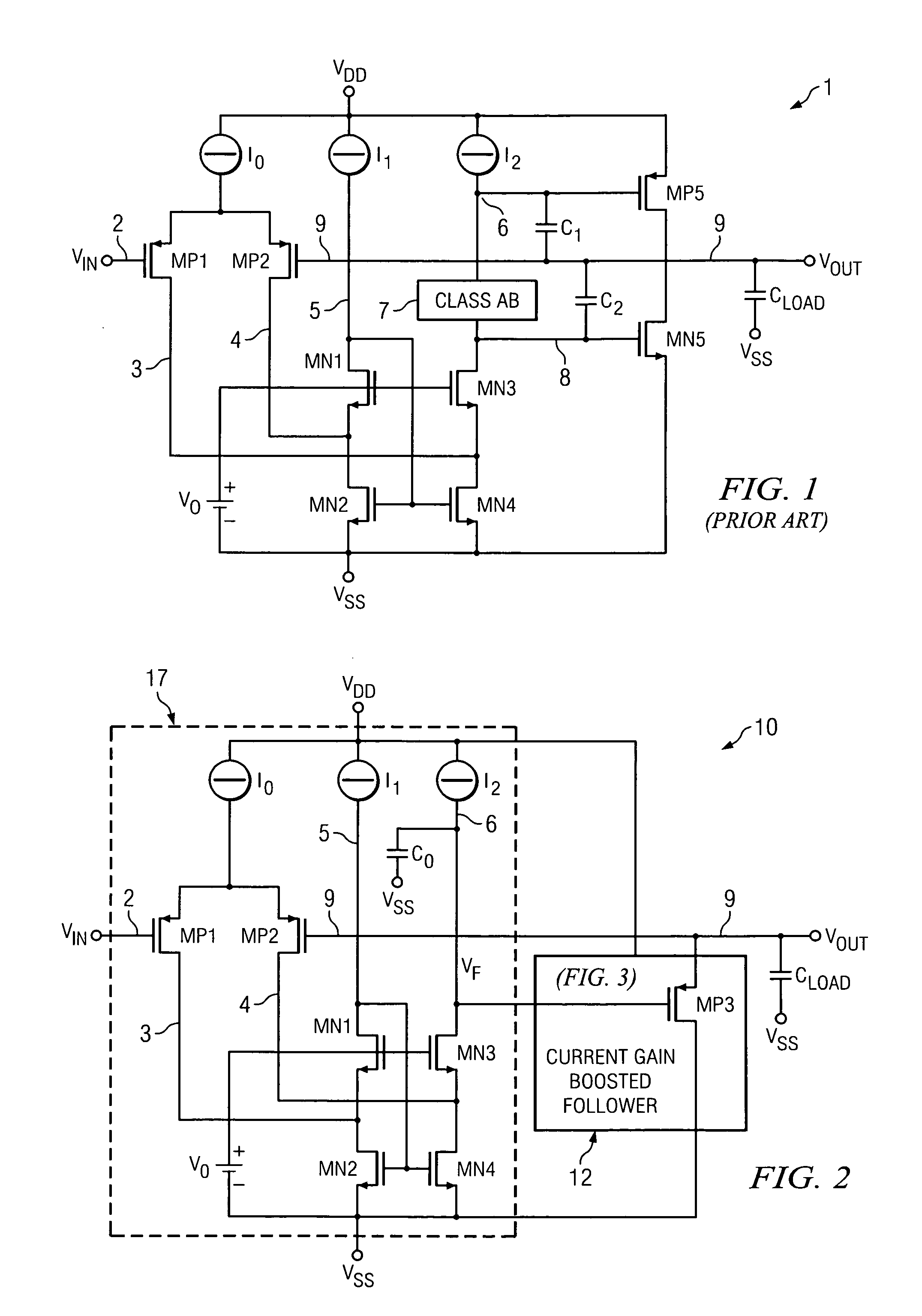
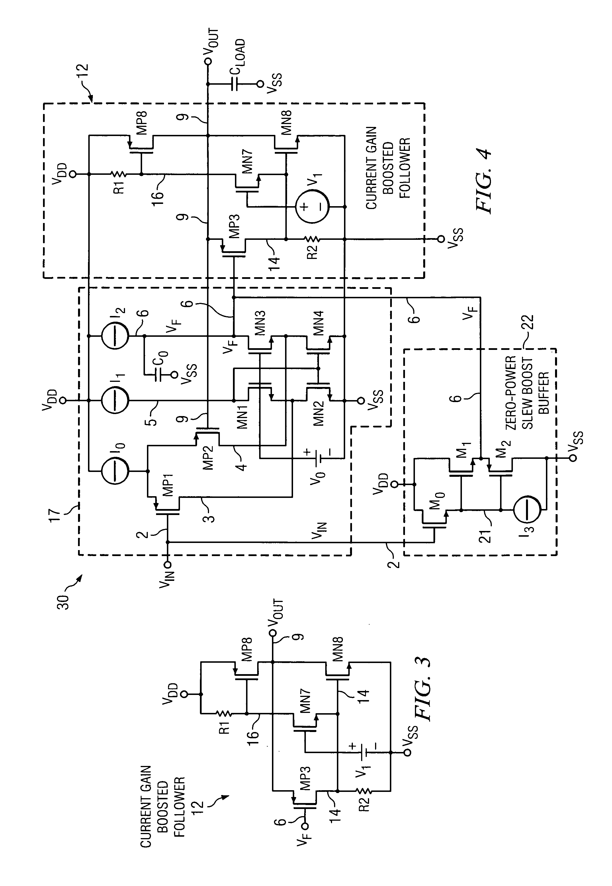
[0035]FIG. 2 is a schematic diagram of a single stage voltage follower amplifier 10. In FIG. 2, voltage follower amplifier circuit 10 includes a differential input stage 17 including P-channel input transistors MP1 and MP2 having their sources coupled to one terminal of a tail current source IO, the other terminal of which is connected to VDD. The gate of input transistor MP1 is connected by conductor 2 to receive an input voltage VIN. The gate of input transistor MP2 is connected to the output signal VOUT. on output conductor 9. The drain of input transistor MP1 is connected by conductor 3 to the junction between N-channel transistor MN2 and N-channel cascode transistor MN1. The drain of input transistor MP2 is connected by conductor 4 to the junction between N-channel transistor MN4 and N-channel cascode transistor MN3. The sources of transistors MN2 and MN4 are connected to VSS. The gates of cascode transistors MN1 and MN3 are connected to a voltage source V0. The gates of lower ...
PUM
 Abstract
Description
Claims
Application Information
 - R&D Engineer
- R&D Manager
- IP Professional
- Industry Leading Data Capabilities
- Powerful AI technology
- Patent DNA Extraction
Browse by: Latest US Patents, China's latest patents, Technical Efficacy Thesaurus, Application Domain, Technology Topic, Popular Technical Reports.
© 2024 PatSnap. All rights reserved.Legal|Privacy policy|Modern Slavery Act Transparency Statement|Sitemap|About US| Contact US: help@patsnap.com


