Flip-flop circuit, semiconductor device and electronic apparatus

Inactive Publication Date: 2013-04-04
NAT UNIV KYOTO INST OF TECH
View PDF1 Cites 3 Cited by
  • Summary
  • Abstract
  • Description
  • Claims
  • Application Information

AI Technical Summary

Benefits of technology

[0035]As described above, a flip-flop circuit of the present invention, for retaining input data, includes: a first master latch circuit for latching the input data; a second master latch circuit for latching the input data; a first C-element circuit for receiving an inverted output of the first master latch circuit and an inverted output of the second master latch circuit; a second C-element circuit for receiving a non-inverted output of the first master latch circuit and a non-inverted output of the second master latch circuit; a first slave latch circuit for latching an output of the first C-element circuit; a second slave latch circuit for latching an output of the second C-element circuit; a third C-element circuit for receiving an inverted output of the first slave latch circuit and an inverted output of the second slave latch circuit; a fourth C-element circuit for receiving a non-inverted output of the first slave latch circuit and a non-inverted output of the second slave latch circuit; a first inverter circuit; a second inverter circuit being interconnected to the first inverter circuit; a third inverter

Problems solved by technology

The more delicate a process has become, the more the number of transient errors has become.
A soft error was a problem related to outer space or an SRAM.
A main cause of generation of a soft error on earth is a high-energy neutron.
In a case where a chip employing one million FFs is used, one error might occur in approximately 100 years.
In the case of SET, an error occurs in such a manner that a pulse is taken by a latch circuit.
However, in order to build a circuit having a high resistance to a soft error, it is necessary to have countermeasures against not only an error due to SEU but also an error due to SET.
However, the flip-flop circuit FF 60 has a pro

Method used


Image

  • Flip-flop circuit, semiconductor device and electronic apparatus
  • Flip-flop circuit, semiconductor device and electronic apparatus
  • Flip-flop circuit, semiconductor device and electronic apparatus

Examples


embodiment 1

[0060]One embodiment of the present invention is described below with reference to FIGS. 1 through 21.

(Configuration of Flip-Flop Circuit of the Present Embodiment)

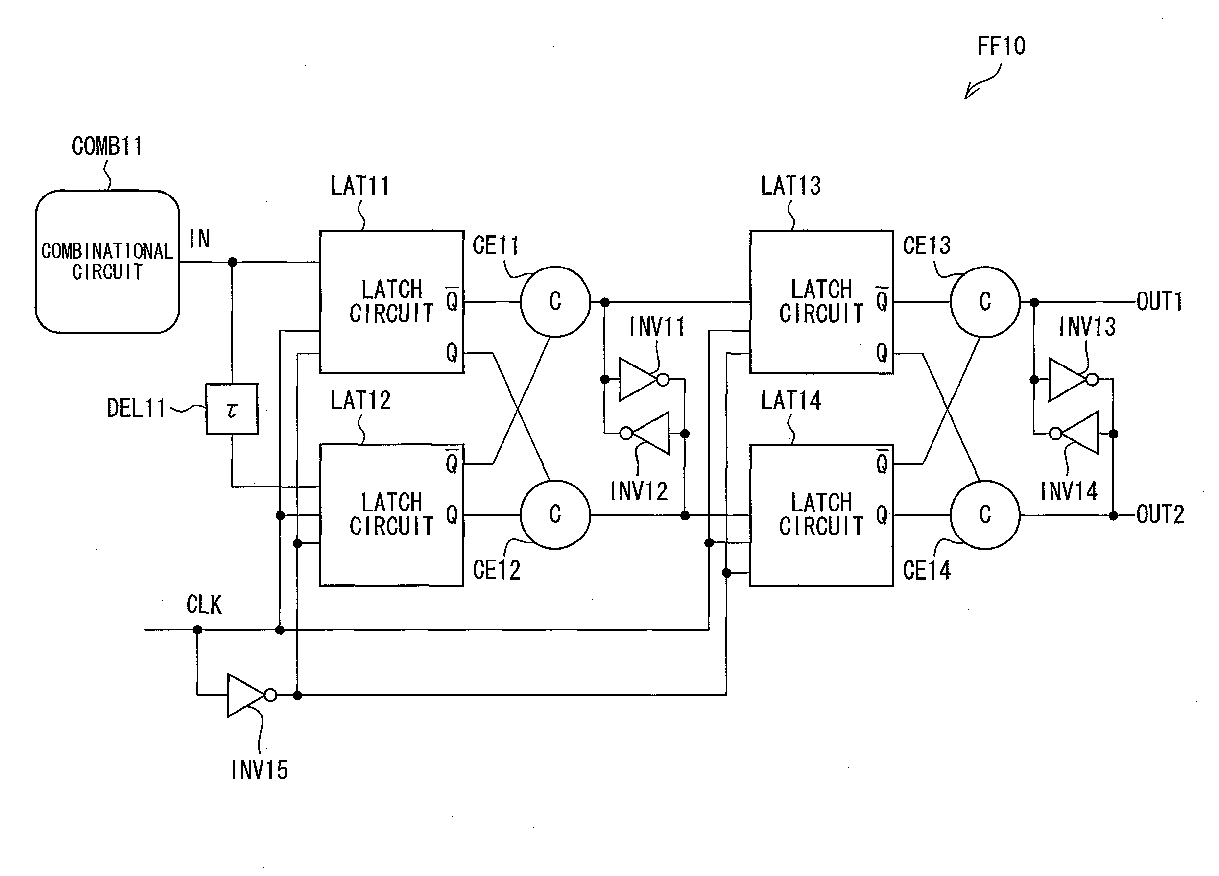
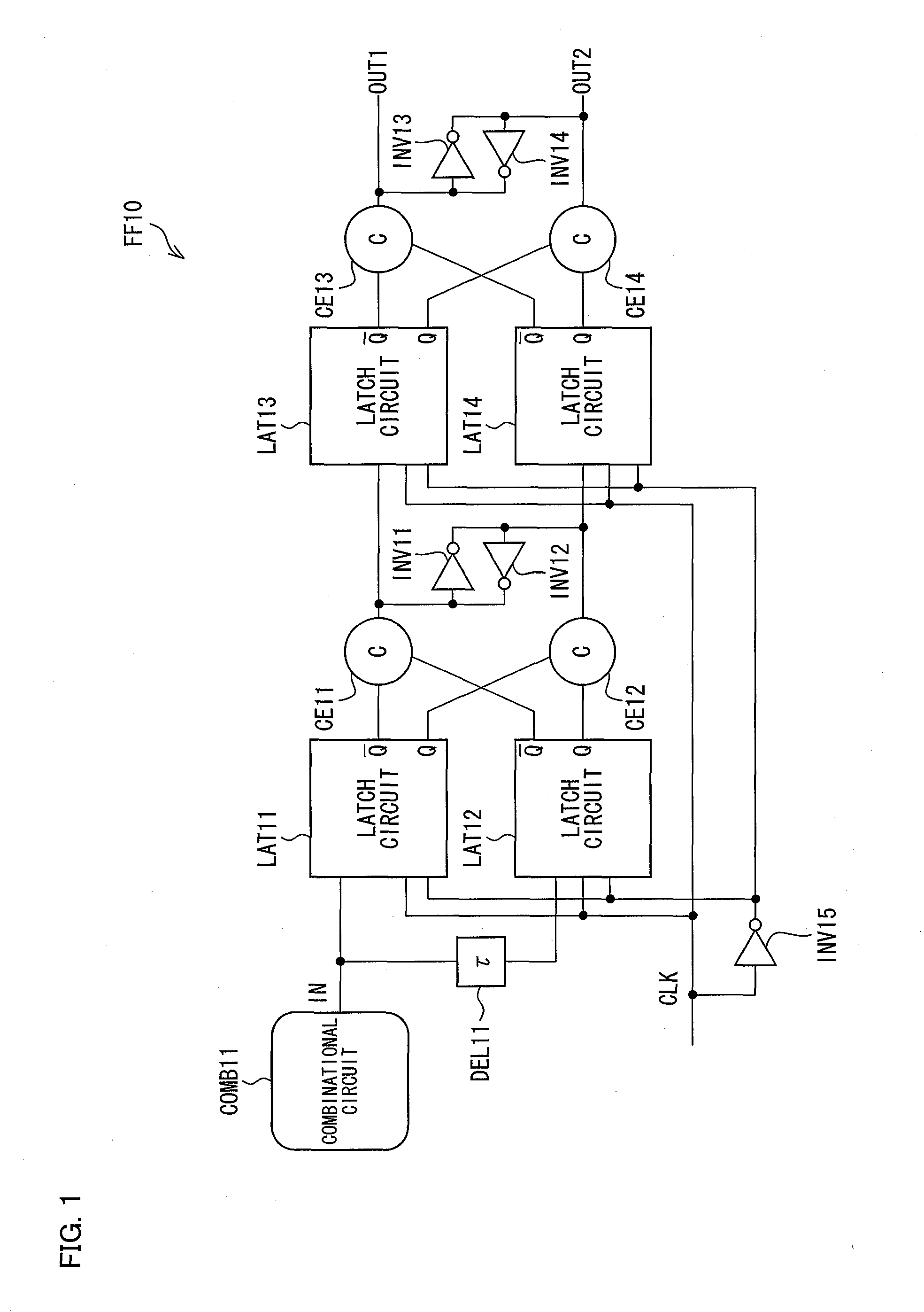
[0061]FIG. 1 is a view illustrating a configuration of a flip-flop circuit FF 10 of the present embodiment. The flip-flop circuit FF 10 is a flip-flop circuit that retains input data IN supplied from a combinational circuit COMB 11. The flip-flop circuit FF 10 includes (i) two master latch circuits LAT 11 and LAT 12, (ii) two slave latch circuits LAT 13 and LAT 14, (iii) four C-element circuits CE 11, CE 12, CE 13, and CE 14, (iv) five inverter circuits INV 11, INV 12, INV 13, INV 14, and INV 15, and (v) a delay circuit DEL 11.

[0062]The master latch circuits LAT 11 and LAT 12 correspond to a first master latch circuit and a second master latch circuit recited in Claims, respectively. An input terminal of the master latch circuit LAT 11 receives input data IN from the combinational circuit COMB 11. Further, an input termin...

example 1

[0081]In order to prove that a flip-flop circuit of the present invention has a higher resistance to an error than that of a conventional flip-flop circuit, the following experiment was carried out.

[0082]As illustrated in FIG. 7, eight flip-flop circuits FF 10 of the present invention were cascade-connected to each other, so as to constitute a shift register. Two selector circuits SEL 11 and SEL 12 were connected to a flip-flop circuit FF 10 provided at a first stage. One of input terminals of the selector circuit SEL 11 received an input signal SI, and one of input terminals of the selector circuit SEL 12 received an inverted input signal bar SI. Moreover, the other one of input terminals of the SEL 11 was connected to one of data output terminals of a flip-flop circuit FF 10 provided at the last stage, and the other one of input terminals of the selector circuit SEL 12 was connected to the other one of data output terminals of the flip-flop circuit FF 10 provided at the last stage...

example 2

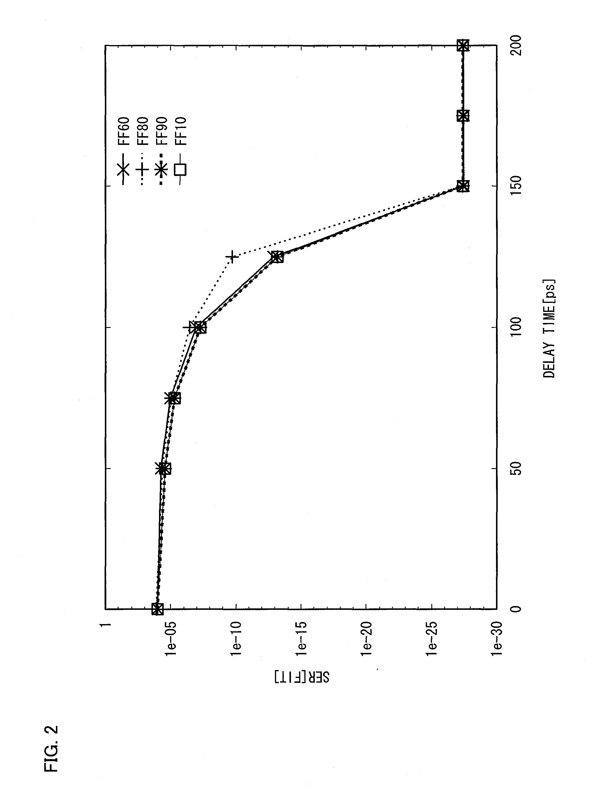
[0090]Further, the inventors of the present invention carried out an experiment in which a shift register was irradiated with a neutron ray. Eight flip-flop circuits FF 10 of the present invention were cascade-connected to each other, so as to constitute a shift register (see FIG. 7). Eight conventional flip-flop circuits FF 90 were cascade-connected to each other, so as to constitute another shift register. Each of the shift registers was irradiated with a neutron ray, and, for each of the shift registers, the number of errors generated in a predetermined time period was counted. As a result, in a case where an operating frequency of the circuits was 100 MHz, the number of errors in the shift register constituted by the flip-flop circuits FF 10 was approximately 31% of the number of errors in the shift register constituted by the flip-flop circuits FF 90. Further, in a case where an operating frequency of the circuits was 10 MHz, the number of errors in the shift register constitut...


PUM


Abstract

A flip-flop circuit (FF 10) of the present invention includes master latch circuits (LAT 11 and LAT 12), slave latch circuits (LAT 13 and LAT 14), C-element circuits (CE 11, CE 12, CE 13, and CE 14), and inverter circuits (INV 11, INV 12, INV 13, and INV 14). The inverter circuits (INV 11 and INV 12) are interconnected to each other between the C-element circuit (CE 11) and the C-element circuit (CE 12). The inverter circuits (INV 13 and INV 14) are interconnected to each other between the C-element circuit (CE 13) and the C-element circuit (CE 14).

Description

TECHNICAL FIELD[0001]The present invention relates to a flip-flop circuit which is increased in resistance to a soft error.BACKGROUND ART[0002]The more delicate a process has become, the more the number of transient errors has become. A typical example of such a transient error is a soft error. A soft error was a problem related to outer space or an SRAM. However, recently, even on earth, it has become necessary to have countermeasures against a soft error. A main cause of generation of a soft error on earth is a high-energy neutron.[0003]As illustrated in FIG. 9, a collision of a high-energy neutron against an Si atom of a substrate generates a secondary ion. In a case where the secondary ion passes by a diffusion layer, electrons or holes gather in the diffusion layer because of (i) diffusion or (ii) occurrence of a drift due to an electric field of a depletion layer. Such electrons or holes change an electric charge of a drain, and, as a result, an output is inverted.[0004]Depend...

Claims


Application Information

Patent Timeline
IPC IPC(8): H03K3/013
CPCH03K3/0375H03K3/013H03K3/3562
Inventor KOBAYASHI, KAZUTOSHIFURUTA, JUNONODERA, HIDETOSHI
Owner NAT UNIV KYOTO INST OF TECH
Why Eureka
Try Eureka