Light emitting diode package and fabrication method thereof

Inactive Publication Date: 2013-04-11
SAMSUNG ELECTRONICS CO LTD
View PDF5 Cites 36 Cited by
  • Summary
  • Abstract
  • Description
  • Claims
  • Application Information

AI Technical Summary

Benefits of technology

[0008]An aspect of the present disclosure provides a light emitting diode (LED) package having reduc

Problems solved by technology

In the related art LED, a dam is formed on a package main body, and an LED chip is then encapsulated (with resin, or the like, held in place by the dam), and he

Method used


Image

  • Light emitting diode package and fabrication method thereof
  • Light emitting diode package and fabrication method thereof
  • Light emitting diode package and fabrication method thereof

Examples


first embodiment

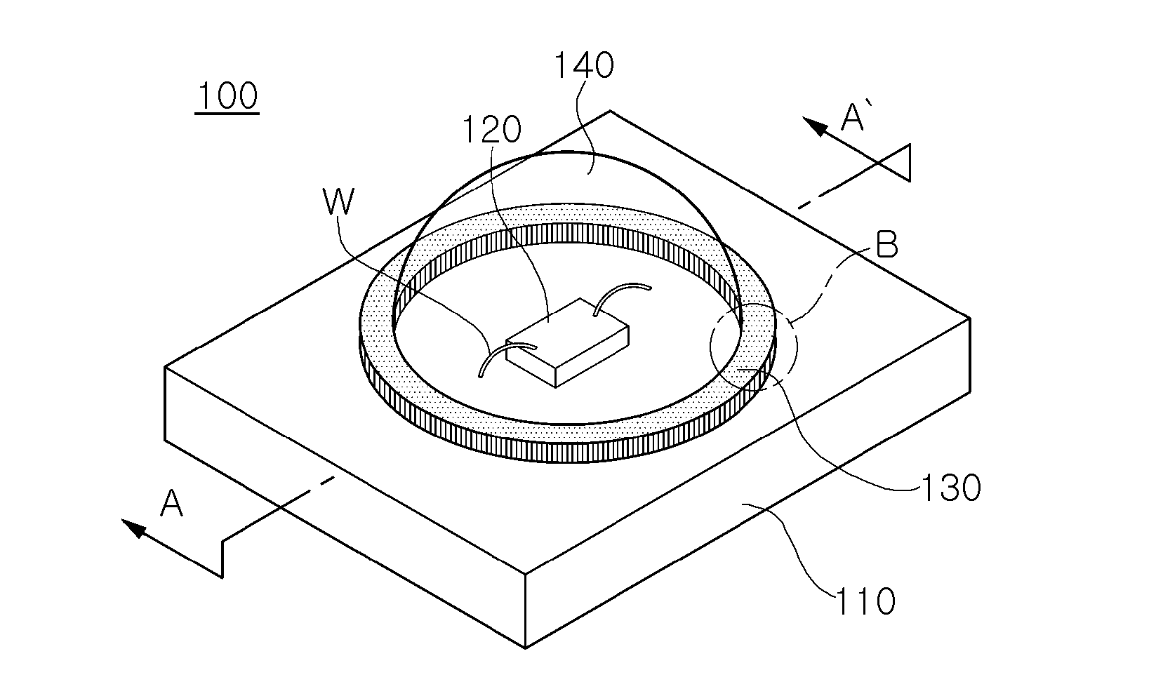
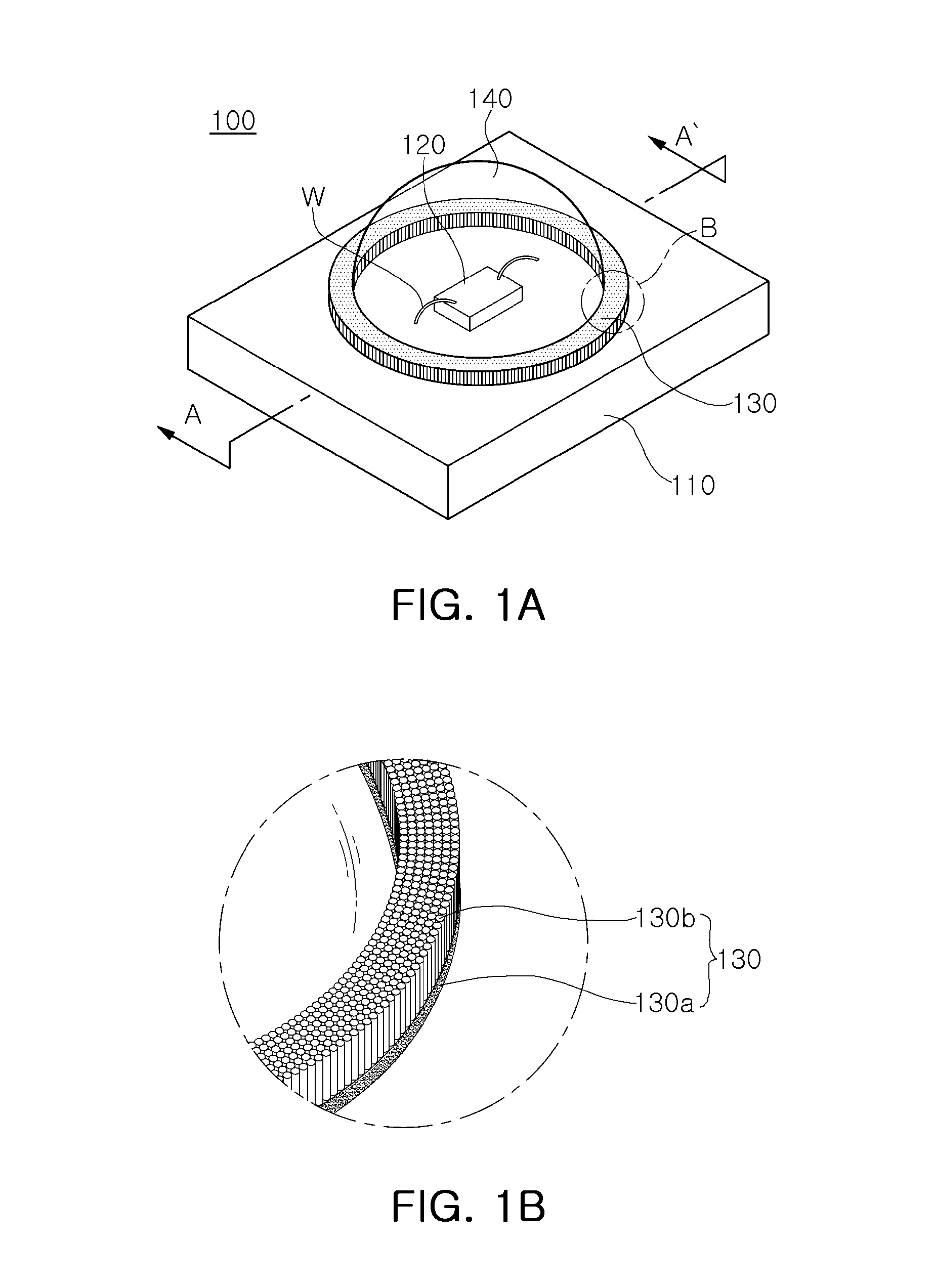
[0054]FIG. 1A is a perspective view schematically showing a light emitting diode (LED) package according to the present disclosure. FIG. 1B is an enlarged view of ‘B’ in FIG. 1A. FIG. 2 is a view schematically showing the section of the LED package illustrated in FIG. 1A taken along line A-A′.

[0055]As shown in FIGS. 1A and 2, an LED package 100 according to a first embodiment of the present disclosure includes a package main body 110, an LED chip 120, a hydrophobic pattern 130, and a resin unit 140.

[0056]The LED chip 120 is mounted on one surface of the package main body 110, and the surface of the package main body 110 on which the LED chip 120 is mounted may be formed to be recessed, with a circumference thereof formed as a sloped face.

[0057]The LED chip 120 is mounted on one surface of the package main body 110 and may be obtained by epitaxially growing a semiconductor layer on a growth substrate. In this case, the growth substrate may be made of sapphire, but the present disclos...

second embodiment

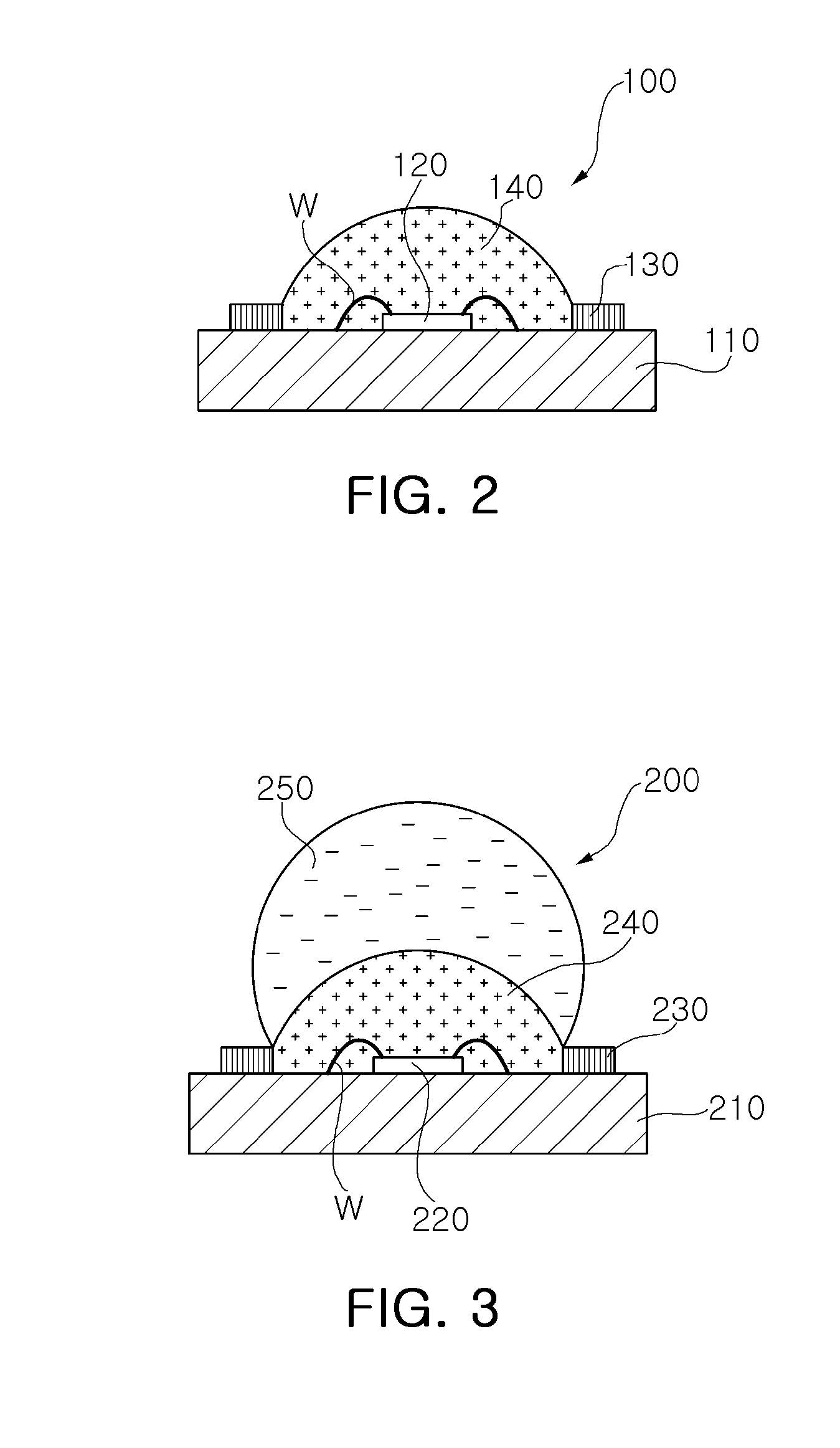
[0082]FIG. 3 is a sectional view schematically showing a light emitting diode (LED) package according to the present disclosure.

[0083]As shown in FIG. 3, the LED package 200 according to a second embodiment of the present disclosure includes a package main body 210, an LED chip 220, a hydrophobic pattern 230, a resin unit 240, and the lens 250.

[0084]Similar to the case as described above, the LED chip 220 is mounted on one surface of the package main body 210, and the surface of the package main body 210 on which the LED chip 220 is mounted may be formed to be recessed with a circumference formed as a sloped face. A hydrophobic pattern 230 is formed to surround the LED chip 220 on the package main body 210. The hydrophobic pattern is formed to have hydrophobicity to serve as a dam defining the resin unit 240 having hydrophilic qualities. The resin 240 encapsulating the LED chip 220 is formed on a region defined by the hydrophobic pattern 230. A component of the resin unit 240 is not...

third embodiment

[0089]As shown in FIG. 4, the LED package 300 according to the present disclosure includes a package main body 310, an LED chip 320, hydrophobic patterns 330 and 330′, a resin unit 340, and a lens 350.

[0090]Similar to the case as described above, the LED chip 320 is mounted on one surface of the package main body 310, and the surface of the package main body 310 on which the LED chip 320 is mounted may be formed to be recessed with a circumference formed as a sloped face.

[0091]Two or more hydrophobic patterns 330 and 330′ are formed in a same manner to surround the LED chip 320. The hydrophobic patterns 330 and 330′ are formed to have hydrophobicity to serve as dams defining the resin unit 340 having hydrophilic qualities. The resin unit 340 encapsulating the LED chip 320 is formed in a region defined by the inner hydrophobic pattern 330, among the two or more hydrophobic patterns, and the lens 350 encapsulating the resin unit 340 is formed in a region defined by the outer hydrophob...


PUM


Abstract

There is provided a light emitting diode (LED) package including: a package main body; an LED chip mounted on the package main body; and a hydrophobic pattern formed on the package main body spaced apart from the LED chip; and a resin unit encapsulating the LED chip and the resin unit is defined by the hydrophobic pattern. The LED package and a fabrication thereof which incur less production costs and have various patterns and enhanced intensity of illumination can be provided.

Description

CROSS-REFERENCE TO RELATED APPLICATIONS[0001]This application claims the priority to Korean Patent Application No. 10-2011-0101741 filed on Oct. 6, 2011, in the Korean Intellectual Property Office, the disclosure of which is incorporated herein by reference.BACKGROUND[0002]1. Field of the Invention[0003]The present invention relates to a light emitting diode package and a fabrication method thereof.[0004]2. Description of the Related Art[0005]A light emitting diode (LED) is a device including a material that emits light by using electrical energy, in which energy generated by electron hole recombination in semiconductor junction parts is converted into light to be emitted therefrom. LEDs are commonly employed as light sources in illumination devices, display devices, and the like, and the development of LEDs has thus been accelerated.[0006]In particular, recently, the development and employment of gallium nitride-based LEDs has been increased, and mobile keypads, side viewers, camer...

Claims


Application Information

Patent Timeline
IPC IPC(8): H01L33/52H01L33/58H01L33/50
CPCH01L2933/005H01L33/54H01L2224/48091H01L2924/12044H01L2924/00014H01L2924/00H01L33/48H01L33/52
Inventor KIM, HAN HYOUNG
Owner SAMSUNG ELECTRONICS CO LTD
Why Eureka
Try Eureka