
Non-volatile memory device and method of operating the same

Active Publication Date: 2013-04-11
SK HYNIX INC
View PDF4 Cites 17 Cited by
  • Summary
  • Abstract
  • Description
  • Claims
  • Application Information

AI Technical Summary

Benefits of technology

The patent relates to a memory device that can speed up its operation by checking the status of multiple groups of pages in a sequential manner and skipping over any failed pages. The result is quicker processing and improved performance. The patent also provides a method for operating this device.

Problems solved by technology

As for the above-described program operation in the conventional non-volatile memory device, when a pass / fail check operation is performed on a plurality of buffer groups in a sequential manner, the pass / fail check operation continues to be performed sequentially until the last region even if a fail has occurred in the first region, thereby resulting in additional operating time.

Method used


Image

  • Non-volatile memory device and method of operating the same
  • Non-volatile memory device and method of operating the same
  • Non-volatile memory device and method of operating the same

Examples


Embodiment Construction

[0020]Hereinafter, various embodiments of the present disclosure will be described in detail with reference to the accompanying drawings. The figures are provided to enable those of ordinary skill in the art to make and use the present invention according to the exemplary embodiments of the present invention. In addition, like or similar reference numerals denote parts performing similar functions and actions throughout the drawings.

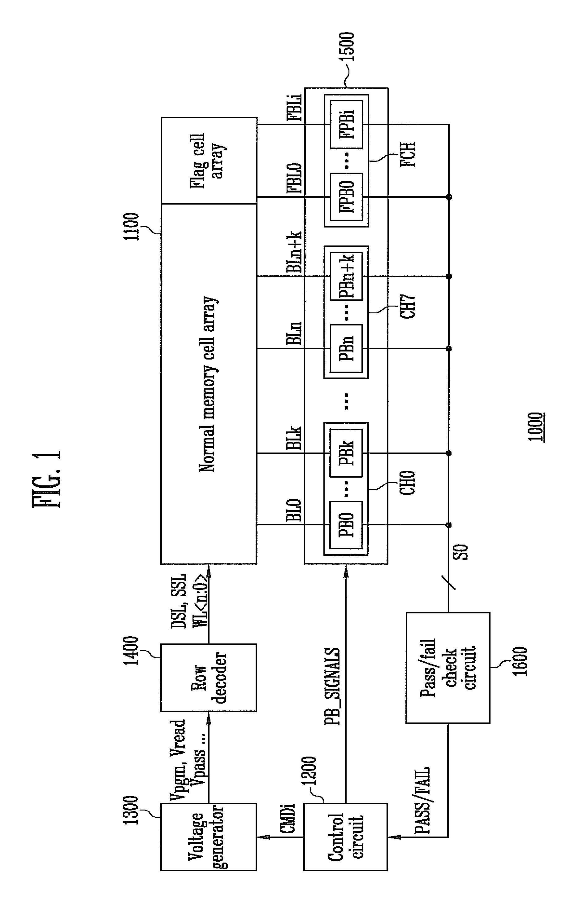
[0021]FIG. 1 is a view illustrating the configuration of a semiconductor memory device according to an embodiment of the present invention.

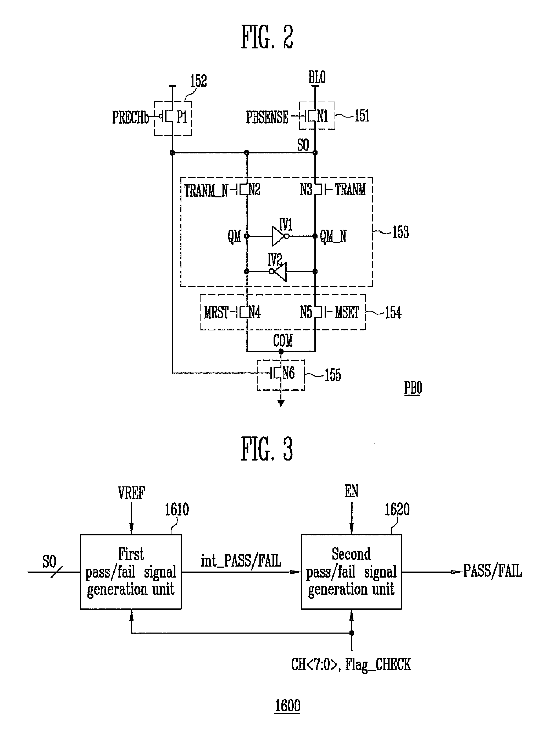
[0022]Referring to FIG. 1, a non-volatile memory device 1000 includes a memory block 1100 having a normal memory cell array and a flag cell array, operation circuits (1300 to 1500) configured to perform a program operation, a read operation and an erase operation for data input and output of memory cells included in a selected page of the memory block 1100, a pass / fail check circuit 1600, and a control circuit 1200 co...


PUM


Abstract

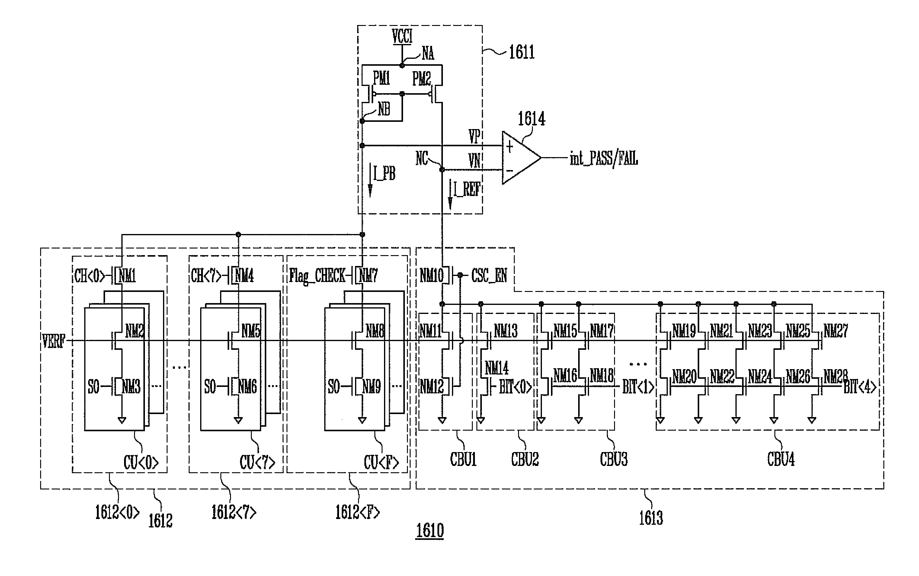
A non-volatile memory device includes a memory cell block including a plurality of memory cells, a plurality of page buffer groups including a plurality of page buffers coupled to bit lines of the memory cell block, a pass / fail check circuit coupled to the plurality of page buffers and configured to perform a pass / fail check operation of comparing a total amount of current varying according to verify data sensed from the memory cells and stored in the page buffers with an amount of reference current corresponding to the number of allowed bits, and a control circuit configured to control the pass / fail check circuit by stopping, when a fail signal is generated during the pass / fail check operation currently being performed on a page buffer group among the plurality of page buffer groups, the pass / fail check operation on the remaining page buffer groups.

Description

CROSS-REFERENCE TO RELATED APPLICATION[0001]Priority is claimed to Korean patent application number 10-2011-0101384 filed on Oct. 5, 2011, the entire disclosure of which is incorporated herein by reference in its entirety.BACKGROUND[0002]1. Field of Invention[0003]Embodiments of the present invention relate to a non-volatile memory device and a method of operating the same, more particularly, to a non-volatile memory device capable of reducing program time and a method of operating the same.[0004]2. Description of Related Art[0005]Recently, non-volatile memory devices that can be electrically programmed and erased and do not require a refresh function for rewriting data at predetermined intervals are in demand.[0006]A non-volatile memory device may apply a program pulse to word lines of memory cells during a program operation and subsequently perform a pass / fail check operation to check whether the memory cells have been programmed or not by using page buffers coupled to the memory ...

Claims


Application Information

Patent Timeline
IPC IPC(8): G11C16/04
CPCG11C16/26G11C16/3459G11C16/06G11C29/00
Inventor KIM, MIN SU
Owner SK HYNIX INC
Learn More