Method of analytical placement with weighted-average wirelength model

a placement algorithm and wirelength technology, applied in computing, instruments, electric digital data processing, etc., can solve the problems of many research challenges, difficult optimization, and difficult modern placement problems, and achieve the effect of limiting the quality of layout results

Active Publication Date: 2013-04-18
NAT TAIWAN UNIV
View PDF4 Cites 220 Cited by
  • Summary
  • Abstract
  • Description
  • Claims
  • Application Information

AI Technical Summary

Benefits of technology

[0015]To improve the deficiency, a force-directed quadratic algorithm is proposed for placing cells and TSVs in a 3D IC. In this algorithm, cells are assigned into multiple dies in a partitioning stage first, and then the placement for cells and the insertion of TSVs are carried out on each die independently for wirelength optimization. To be more specific, cells will not be moved across dies for wirelength optimization during the placement with TSVs. However, this may limit the quality of layout results.

Problems solved by technology

The placement problem is to place objects into one or more fixed dies such that no objects overlap with each other and some cost metric (e.g., wirelength) is optimized.
Although it is a classical problem, many modern design challenges have reshaped this problem.
The modern placement problem becomes very tough because we need to handle large-scale designs.
Since HPWL is not differentiable, it is hard to perform the optimization.
However, the problem with improving analytical modeling for wirelength still induces many research challenges.
The 3D IC technology can effectively reduce global interconnect length and increase circuit performance; however, this technology brings some challenges with through-silicon vias (TSVs), used to make interconnections among different dies (layers), thermal effects, packaging, power delivery / density, etc.
These TSVs are responsible for the interconnections among devices on different layers, but they could cause some significant problems.
Under current technologies, TSV pitches are very large compared to the sizes of regular metal wires; as a result, a large number of TSVs will consume significant silicon areas and degrade the yield and reliability of the final chip.
In addition, TSVs are usually placed at the whitespace among macro blocks or cells, and thus TSVs might affect the routing resource and increase the overall chip or package area.
The significant silicon areas occupied by TSVs and the induced yield and reliability issues become critical problems for 3D IC placement.
As known for the 2D placement problem, however, a partitioning-based approach is not as competitive as an analytical one.
However, since the sizes of TSVs are not considered during placement, the efficiency of the approaches mentioned above is usually not good enough.
However, this may limit the quality of layout results.

Method used


Image

  • Method of analytical placement with weighted-average wirelength model
  • Method of analytical placement with weighted-average wirelength model
  • Method of analytical placement with weighted-average wirelength model

Examples


Embodiment Construction

[0033]The detailed explanation of the present invention is described as following. The described preferred embodiments are presented for purposes of illustrations and description, and they are not intended to limit the scope of the present invention.

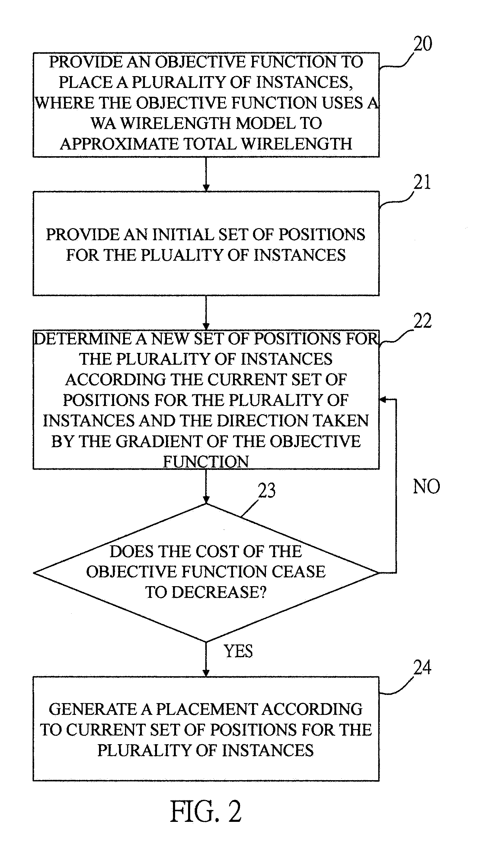
[0034]Typically, the placement problem for an integrated circuit (IC) is solved in three stages (1) global placement, (2) legalization, and (3) detailed placement. Global placement evenly distributes the instances and finds the best position and layer for each instance to minimize the target cost (e.g., wirelength). Then legalization removes all instance overlaps for each layer. Finally, detailed placement refines the placement solution.

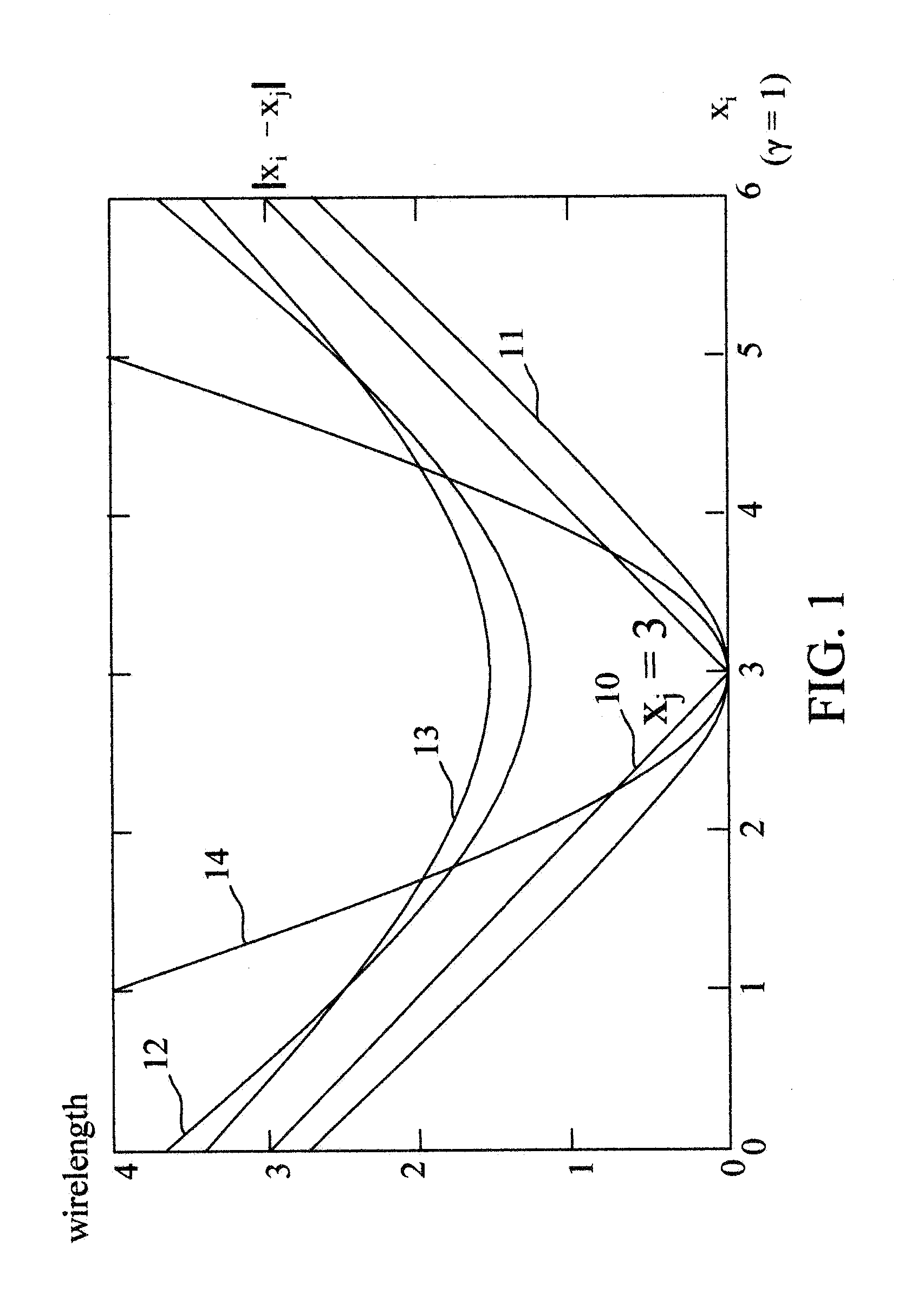
Weighted-Average (WA) Wirelength Model

[0035]In this invention, a novel weighted-average (WA) wirelength model for analytical global placement is presented.

[0036]In general, a placement problem can be formulated as a hypergraph H=(V,E) placement problem. Let V={v1, v2, . . . , vn} represent instances, and ...


PUM


Abstract

A computer-implemented method to generate a placement for a plurality of instances for an integrated circuit (IC) by utilizing a novel weighted-average (WA) wirelength model, which outperforms a well-known log-sum-exp wirelength model, to approximate the total wirelength. The placement is determined by performing an optimization process on an objective function which includes a wirelength function approximated by the WA wirelength model. The method can be extended to generate a placement for a plurality of instances for a three-dimensional (3D) integrated circuit (IC) which considers the sizes of through-silicon vias (TSVs) and the physical positions for TSV insertion. With the physical positions of TSVs determined during placement, 3D routing can easily be accomplished with better routed wirelength, TSV counts, and total silicon area.

Description

BACKGROUND OF THE INVENTION[0001]1. Field of the Invention[0002]The invention relates in general to a computer-implemented method for generating placements for integrated circuits (ICs) and, in particular, to a method for generating placements for integrated circuits (ICs) with an analytical placement algorithm.[0003]2. Description of the Prior Art[0004]The placement problem is to place objects into one or more fixed dies such that no objects overlap with each other and some cost metric (e.g., wirelength) is optimized. Placement is a major step in physical design that has been studied for several decades. Although it is a classical problem, many modern design challenges have reshaped this problem. The modern placement problem becomes very tough because we need to handle large-scale designs.[0005]In modern placement algorithms, analytical placement algorithms have been shown to be most effective for large-scale IC designs. Analytical placement formulates the placement problem as math...

Claims


Application Information

Patent Timeline
Patent Type & Authority Applications(United States)
IPC IPC(8): G06F17/50
CPCG06F17/5072G06F30/392
Inventor BALABANOV, VALERIYHSU, MENG-KAICHANG, YAO-WEN
Owner NAT TAIWAN UNIV
Why Eureka
Try Eureka