

Lead frame for optical semiconductor device, method of producing the same, and optical semiconductor device
a technology of optical semiconductor and lead frame, which is applied in the direction of semiconductor/solid-state device details, optical elements, optics, etc., can solve the problems of red color system rendering property and inability to avoid lowering reflectance, and achieve satisfactory reflection characteristics, excellent reflection characteristics, and satisfactory reflectance
- Summary
- Abstract
- Description
- Claims
- Application Information
AI Technical Summary
Benefits of technology
Problems solved by technology
Method used
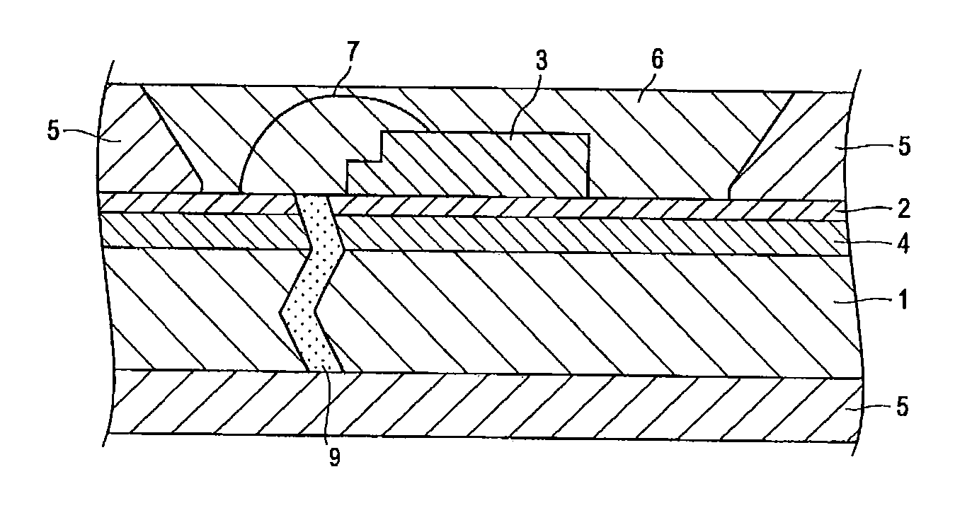
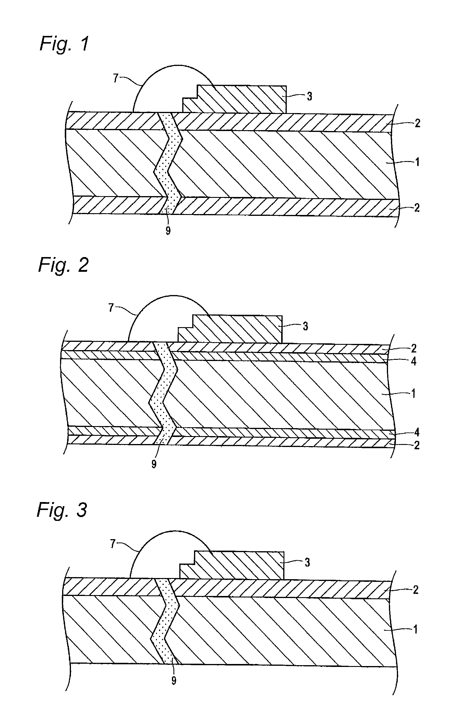
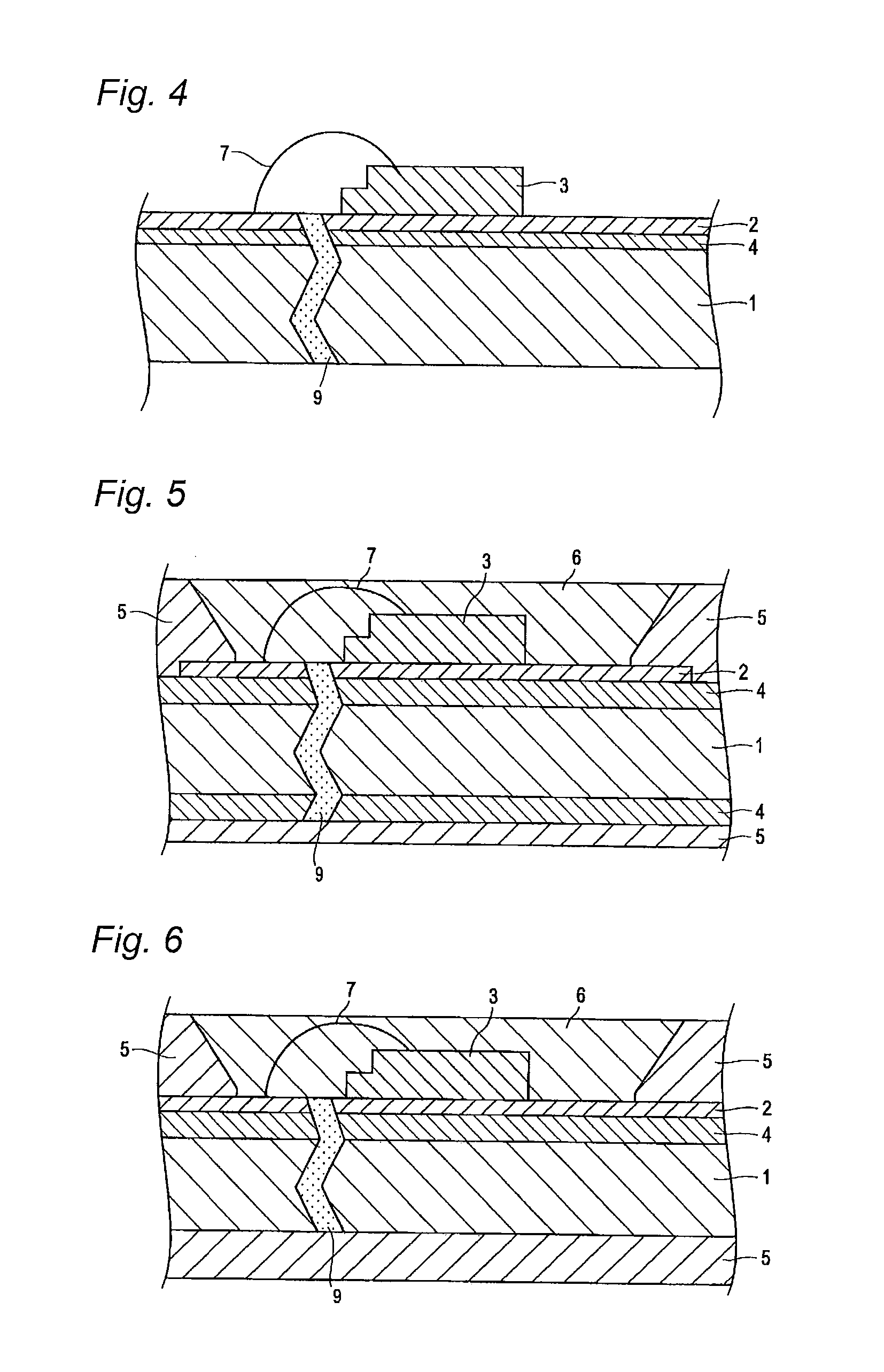
Image

Examples
example 1
[0146]As Example 1, substrates with width 100 mm, as shown in Table 1, were subjected to the respective pretreatment as shown below, followed by electroplating as shown below. Then, on the resultant substrates, reflection layers were initially formed by plating, by changing the sheet thickness upon initial formation of the reflection layer (upon plating), taking into consideration the working ratio at the time of rolling after the formation of the reflection layer, so that the total sheet thickness including the coating thickness after rolling would be 0.2 mm. Then, the thus-plated substrates were subjected to rolling to thickness 0.2 mm at the respective area reduction ratio as shown in Table 1, using a 6-stage rolling machine (manufactured by Hitachi, Ltd.), with rolls in which rolling work rolls had the surface roughness Ra of approximately 0.03 μm, to obtain samples (rolling finished products) of Examples 1 to 38 and Reference Examples 1 to 3, having the structures as shown in T...
example 2
[0193]As Example 2, substrates with width 100 mm, as shown in Table 3, were subjected to the respective pretreatment in the same manner as in Example 1, followed by electroplating, as shown in Table 3, in the same manner as in Example 1. That is, substrates with thickness 0.25 mm or 0.83 mm were used, and each of the substrates was plated with Ag on each side such that the Ag coating thickness after rolling would be 3 μm. Then, the resultant substrate was subjected to rolling at a working ratio of 40% at the time of rolling after the formation of the reflection layer, to obtain strips with thicknesses 0.15 mm or 0.5 mm, respectively. Then, the strips were subjected to punching with a press, followed by electroplating, to form a plating coating favorable in solder wettability, only in the external lead section, by means of a resist mask, and removing the resist, to obtain Examples 39 to 50 and Reference Examples 6 to 9, having the structures as shown in Table 3, respectively.
[0194]Fu...
example 3
[0212]This is an example of the embodiment characterized by the plating microstructure residual ratio.
[0213]As Example 3, electric conductive substrates, as shown in Table 5, with thickness 0.25 mm and width 180 mm, were subjected to the respective pretreatment in the same manner as described above, followed by electroplating in the same manner as described above. Then, in order to cause plastic deformation to the resultant Ag plating layer, the Ag plated substrates were subjected to rolling or pressing, with changing the working ratio, to obtain lead frames of Examples 101 to 121 and Reference Examples 101, respectively. Reference Example 102 was a simulation of Comparative Example 1 of Patent Literature 3, and Reference Example 103 was a simulation of Example 2 of Patent Literature 3, respectively, and those samples were provided by rolling, followed by a heat treatment at 240° C. for 4 hours (heat treatment finished products). In Conventional Example 101, an electric conductive s...
PUM
| Property | Measurement | Unit |
|---|---|---|
| surface roughness Sa | aaaaa | aaaaa |
| surface roughness Ra | aaaaa | aaaaa |
| thickness | aaaaa | aaaaa |
Abstract
Description
Claims
Application Information