Light emitting diode component

a technology of light-emitting diodes and components, which is applied in the manufacture of electrode systems, electric discharge tubes/lamps, and discharge tubes luminescent screens, etc., can solve the problems of increasing the complexity and cost of led components, and achieve the effects of reducing the roughness of this layer, increasing the complexity and cost of led components, and improving extraction

Active Publication Date: 2013-04-25
COMMISSARIAT A LENERGIE ATOMIQUE ET AUX ENERGIES ALTERNATIVES
View PDF7 Cites 21 Cited by
  • Summary
  • Abstract
  • Description
  • Claims
  • Application Information

AI Technical Summary

Benefits of technology

[0013]In this way the combination of the encapsulation layer and the reflection layer makes it possible to form an interface capable of extracting outside the light-emitting diode all or part of the secondary radiation being propagated toward the primary source or the inside of the LED component. The secondary radiation blocked and reflected toward the outside by the said interface comes from the secondary source either directly or by reflection.
[0025]the conversion layer is disposed in contact with the reflection layer. The method comprises a step of increasing the roughness at the interface between the conversion layer and the reflection layer. This roughness Ra preferably is greater than 50 nm. In this way the method according to the invention makes it possible to impart a diffusing nature to this interface.

Problems solved by technology

In the context of this invention, it turned out that this modification of the conversion layer leads to an increased achievement complexity and cost for the LED component.

Method used


Image

  • Light emitting diode component
  • Light emitting diode component
  • Light emitting diode component

Examples


Embodiment Construction

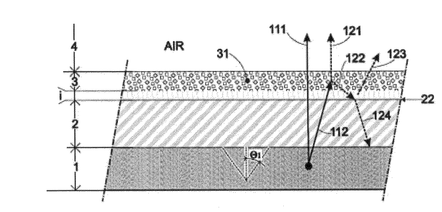
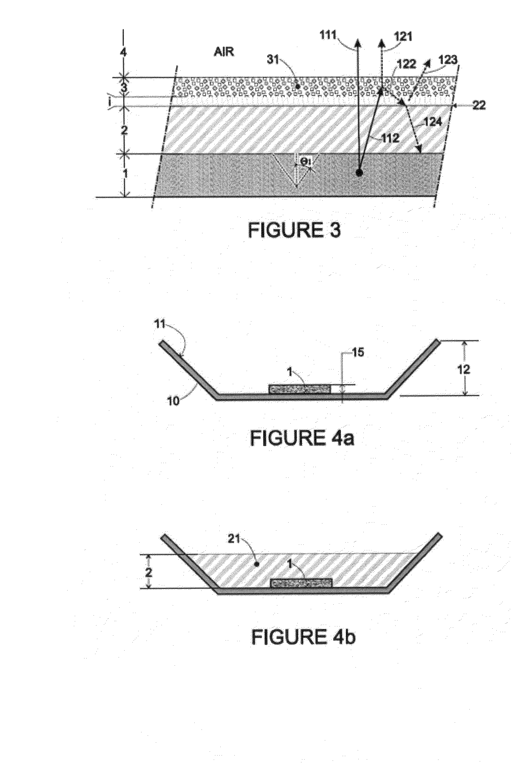
[0035]Before undertaking a detailed review of the embodiments of the invention, optional characteristics which may be used in combination or alternatively, if need be, are set forth below:[0036]The said face of the reflection layer has a roughness Ra less than 50 nm and preferably less than 5 nm. The roughness Ra is defined as the mean arithmetic deviation. It is usually measured by means of an atomic force microscope (AFM) for example.[0037]The index of refraction ni of the reflection layer is greater than the index n2 of the encapsulation layer. The reflection layer and the encapsulation layer preferably are configured so that ni / n2>1.2. Even more preferentially, the reflection layer and the encapsulation layer are configured so that ni / n2>1.4.

[0038]By using only the characteristics (indexes of refraction and roughness in particular) of the intermediate layer and the encapsulation layer, it is possible in this way to achieve a specular or almost specular behavior at the said inter...


PUM

PropertyMeasurementUnit
roughness Raaaaaaaaaaa
thicknessaaaaaaaaaa

Abstract

A light-emitting diode component includes a primary source, a conversion layer forming a secondary source configured for absorbing the primary radiation at least in part and emitting a secondary radiation, an encapsulation layer, situated between the primary and secondary sources. The light-emitting diode component also includes a reflection layer (i) situated between the encapsulation layer and the conversion layer and having a face in contact with the encapsulation layer so as to form an interface with the encapsulation layer, the reflection layer (i) and the encapsulation layer being configured so that the interface allows the primary radiation originating from the primary source to pass and reflects the secondary radiation toward the outside of the light emitting diode.

Description

TECHNICAL FIELD OF THE INVENTION[0001]This invention relates to light-emitting diodes in general and more particularly to those that are designed to emit a light from a primary source and from a secondary source which absorbs a part of the radiation from the primary source and which reemits its own radiation. This application covers for example for application light-emitting diodes emitting a white light.STATE OF THE ART[0002]Light-emitting diodes, or LED, acronym for the English “light-emitting diode,” produced since the sixties by the microelectronics industry have seen their field of application broaden with the passing years. Lighting, as replacement for incandescent lamps, and more sophisticated applications such as backlighting for liquid crystal displays, now form part of the field of application of LEDs. These applications require being able to have white LEDs. By the very fact of the physical operating principle of LEDs, there is, however, no single diode capable of emittin...

Claims


Application Information

Patent Timeline
Patent Type & Authority Applications(United States)
IPC IPC(8): H05B33/12H05B33/10
CPCH05B33/10H05B33/12H01L33/52H01L33/507H01L33/46
Inventor GASSE, ADRIENDESIERES, YOHANLEVY, FRANCOIS
Owner COMMISSARIAT A LENERGIE ATOMIQUE ET AUX ENERGIES ALTERNATIVES
Why Eureka
Try Eureka