Method for producing a photovoltaic module having backside-contacted semiconductor cells, and photovoltaic module

a photovoltaic module and semiconductor technology, applied in the field of photovoltaic modules with backside contact semiconductor cells, can solve the problems of hammering an efficient large-scale production of such modules, and achieve the effect of achieving good manufacturing tolerances

Inactive Publication Date: 2013-05-02
SOLARWORLD IND THURINGEN
View PDF7 Cites 5 Cited by
  • Summary
  • Abstract
  • Description
  • Claims
  • Application Information

AI Technical Summary

Benefits of technology

[0011]One great advantage of the method is that positional inaccuracies in the placement of the semiconductor cells, which sometimes occur in large-scale manufacturing processes, do not cause any problem. The actual locations of the contacting areas between the semiconductor cells and the conductive substrate coating are specified only when the contacting is imminent. This makes it possible to allow the placement process of the semiconductor cells to take place at relatively generous manufacturing tolerances.
[0012]In one specific embodiment, a lamination step for laminating the semiconductor cells is expediently implemented after the semiconductor cells have been placed on the substrate. This permanently joins the semiconductor cells to the substrate, thereby preventing them from changing their positions during subsequent method steps. In addition, the entity made up of the substrate and the laminated semiconductor cells forms a composite, which is able to be stored and held in readiness for the subsequent method steps without any problems.

Problems solved by technology

The difficulties this entails with regard to the precise positioning of the semiconductor cells in a given cell arrangement have the result that the backside contacting, which is advantageous with regard to the energy yield of the photovoltaic module, requires a complicated manufacturing process, which, above all, hampers an efficient large-scale production of such modules.

Method used


Image

  • Method for producing a photovoltaic module having backside-contacted semiconductor cells, and photovoltaic module
  • Method for producing a photovoltaic module having backside-contacted semiconductor cells, and photovoltaic module
  • Method for producing a photovoltaic module having backside-contacted semiconductor cells, and photovoltaic module

Examples


Embodiment Construction

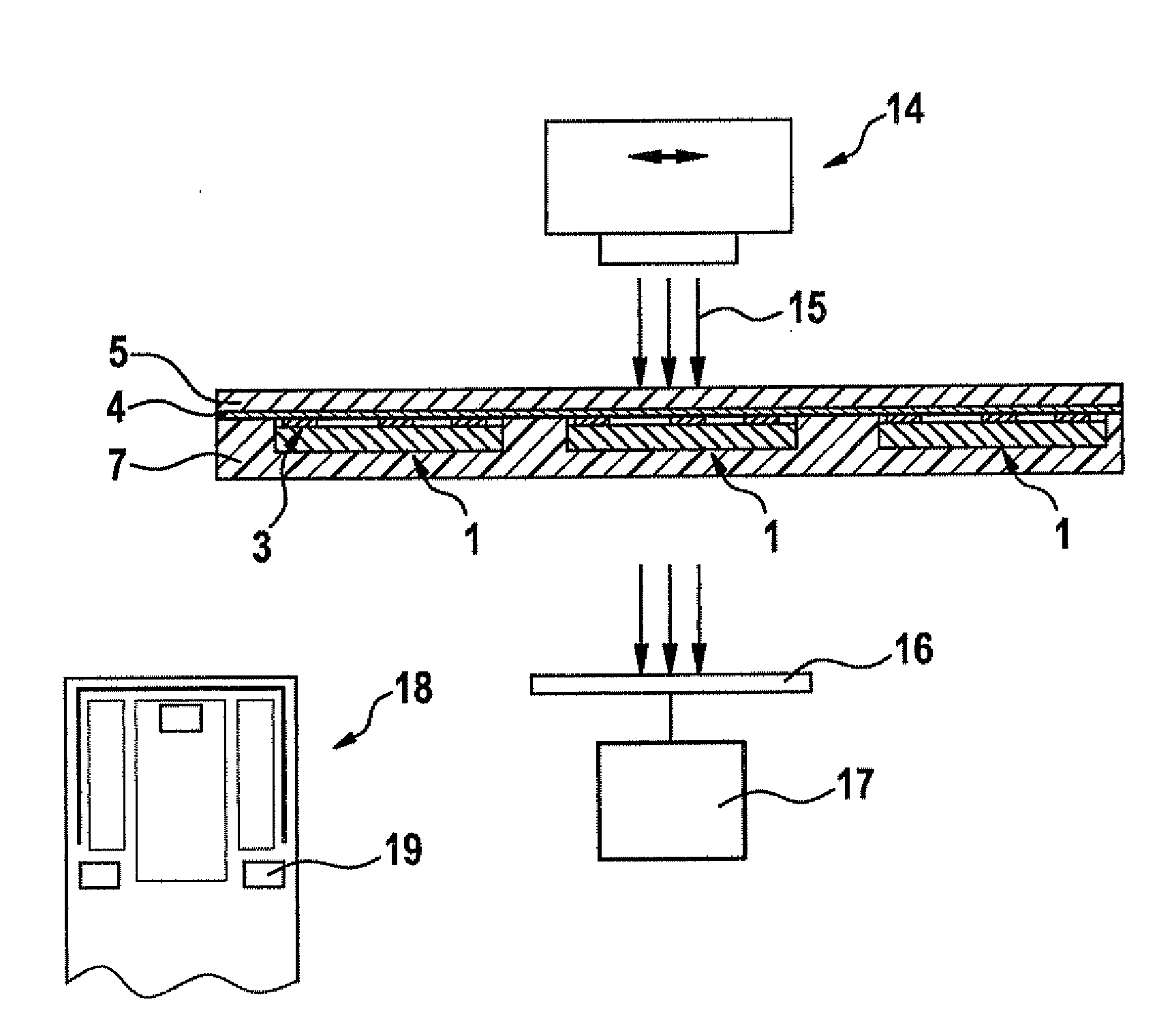
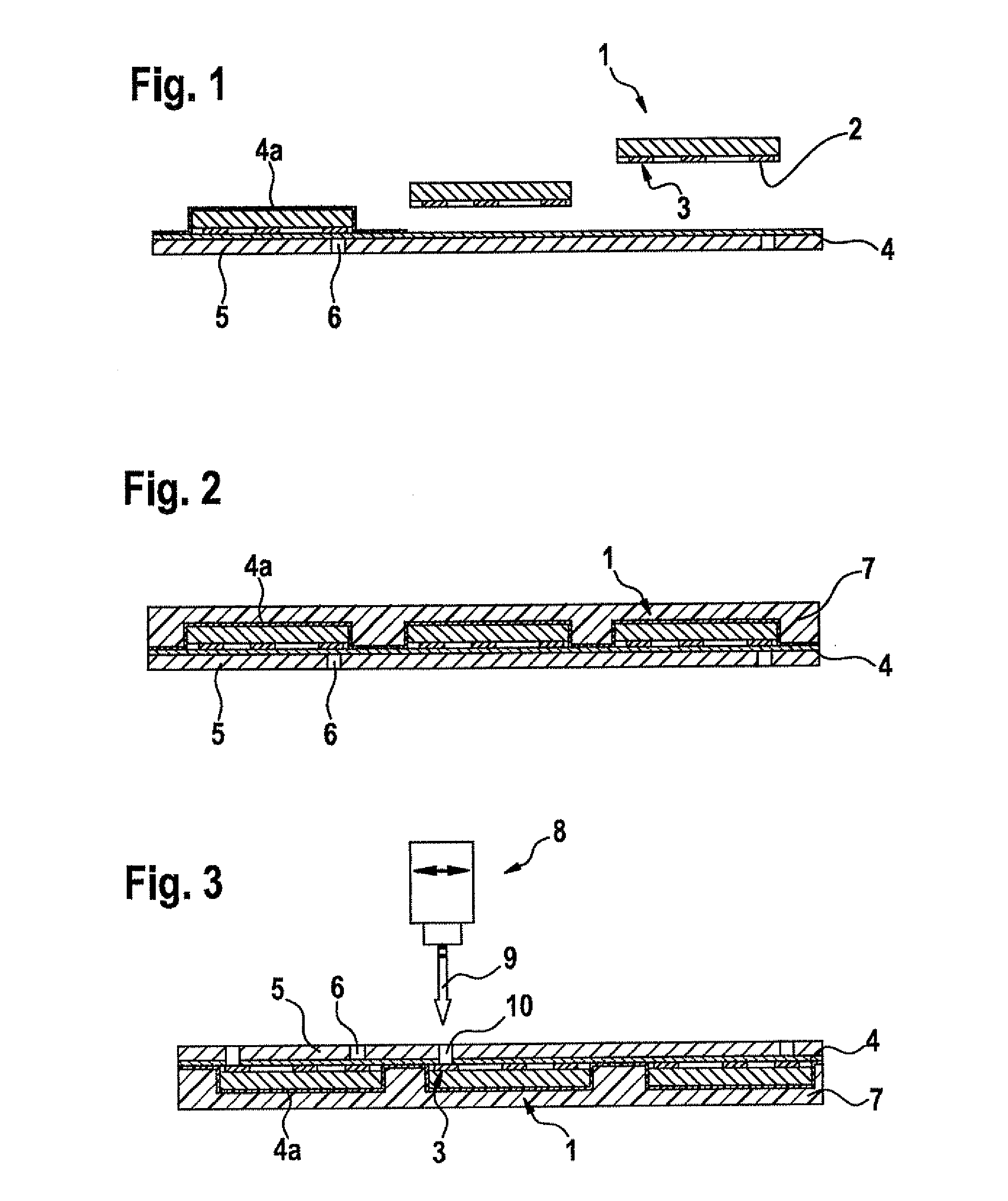
[0030]FIG. 1 shows a placement step for semiconductor cells on a substrate. Semiconductor cells 1 shown here are developed as crystalline photovoltaic cells, for instance. They are made of silicon or a comparable semiconductor material and include the doped regions (not shown here in detail) for the energy conversion of solar energy into electrical voltage. Each semiconductor cell has a contact side 2 which features contact regions 3 disposed thereon. The contact regions usually are galvanically metallized. A placement device, which is not shown here, is normally used for the placement.

[0031]A substrate 4 is provided for the backside contacting of the semiconductor cells and, in particular, their contact sides 2. This substrate is made of a foil-type, electrically insulating material or a laminate of electrically non-conductive foils. The fixation of the semiconductor cells on the substrate is accomplished by means of a plastic foil 4a. This foil is made of, for example, ethylene vi...


PUM


Abstract

A method for producing a photovoltaic module having backside-contacted semiconductor cells which have contact regions provided on a contact side includes: providing a foil-type, non-conducting substrate having an at least one-sided and at least sectionally electrically conductive substrate coating on a first substrate side; placing the contact sides of the semiconductor cells on a second substrate side; implementing a local perforation which penetrates the substrate and the substrate coating, to generate openings at the contact regions of the semiconductor cells; applying a contact element to fill the openings and to form a contact point between the substrate coating on the first substrate side and the semiconductor cells on the second substrate side.

Description

BACKGROUND OF THE INVENTION[0001]1. Field of the Invention[0002]The present invention relates to a method for producing a photovoltaic module having backside-contacted semiconductor cells, and to a photovoltaic module.[0003]2. Description of the Related Art[0004]Photovoltaic modules based on semiconductors known from the related art are made up of a totality of semiconductor cells. Under the influence of external incident light an electrical voltage is produced inside these cells. The semiconductor cells are expediently interconnected so that the highest possible current intensity can be picked off at the photovoltaic module. This requires contacting of the semiconductor cells and expedient line wiring within the photovoltaic module.[0005]The known photovoltaic modules use what is known as ribbons for the wiring and cabling. Usually, these are conductor segments made of metal, especially copper, which are developed in the form of strips. The contacting between a ribbon and the semic...

Claims


Application Information

Patent Timeline
Patent Type & Authority Applications(United States)
IPC IPC(8): H01L31/05
CPCH01L21/268H01L31/022433Y02E10/547H01L31/1804H01L31/0516H01L31/05Y02P70/50H01L31/0224H01L31/18
Inventor KOYUNCU, METINSCHAAF, ULRICHKUGLER, ANDREASZERRER, PATRICKZIPPEL, MARTINSTIHLER, PATRICK
Owner SOLARWORLD IND THURINGEN
Why Eureka
Try Eureka