Fast, High Resolution 3-D Flash LADAR Imager
a high-resolution, 3d flash technology, applied in the field of electronic circuits, can solve the problems of inconvenient use, inconvenient use, and high cost of coherent laser sources, and achieve the effects of reducing the range resolution of these forms of systems, and increasing the cost of receiver systems
- Summary
- Abstract
- Description
- Claims
- Application Information
AI Technical Summary
Benefits of technology
Problems solved by technology
Method used
Image
Examples
Embodiment Construction
[0049]Prior art photodetector sensor read out integrated circuits (or “ROICs”) used in existing LADAR imaging circuitry are constrained in functionality due to small unit cell size, power demands, speed and complexity. Fortunately, high density microelectronic integrated circuit (“IC”) chip stacking technology such as by Irvine Sensors Corp., assignee herein, provides ROIC design options with enhanced flexibility by offering greatly increased ROIC circuit element density than is provided in prior art, non-stacked design solutions.
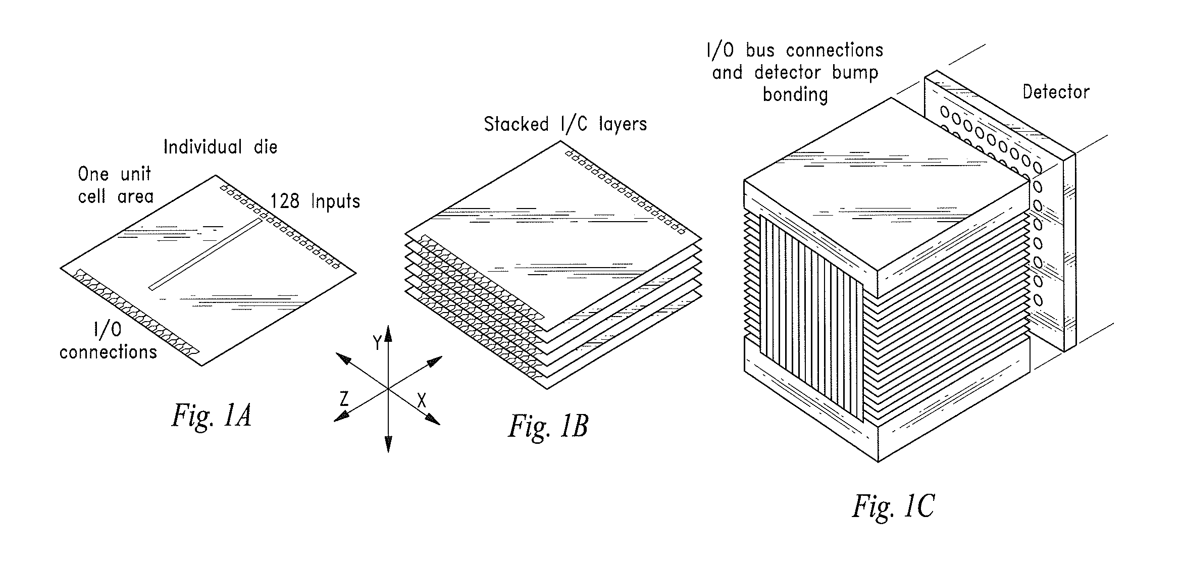
[0050]An exemplar LADAR imaging module architecture incorporating the stacked IC chip technology referred to above is shown in FIGS. 1A, 1B and 1C and is disclosed in, for instance, U.S. Pat. No. 7,436,494 entitled “Three-Dimensional LADAR Module With Alignment Reference Insert Circuitry” to Kennedy et al. and issued on Oct. 14, 2008.
[0051]FIG. 1a shows an IC layer having a unit cell with a circuit of the invention fabricated thereon and having I / O connecti...
PUM
 Abstract
Description
Claims
Application Information


