Method of manufacturing semiconductor device

a manufacturing method and semiconductor technology, applied in semiconductor/solid-state device manufacturing, basic electric elements, electric devices, etc., can solve the problem that the impurities which adhered to the substrate before crystal growth cannot be removed

Inactive Publication Date: 2013-05-02
MITSUBISHI ELECTRIC CORP
View PDF5 Cites 2 Cited by
  • Summary
  • Abstract
  • Description
  • Claims
  • Application Information

AI Technical Summary

Benefits of technology

[0009]Other and further objects, features and advantages of the invention will appear more fully from the following description.

Problems solved by technology

The semiconductor device manufacturing method disclosed in the above publication is disadvantageous in that, since the dummy layer is formed on the multilayer structure after forming the structure on the substrate, the impurities which adhered to the substrate before the crystal growth cannot be removed.

Method used


Image

  • Method of manufacturing semiconductor device
  • Method of manufacturing semiconductor device
  • Method of manufacturing semiconductor device

Examples


first embodiment

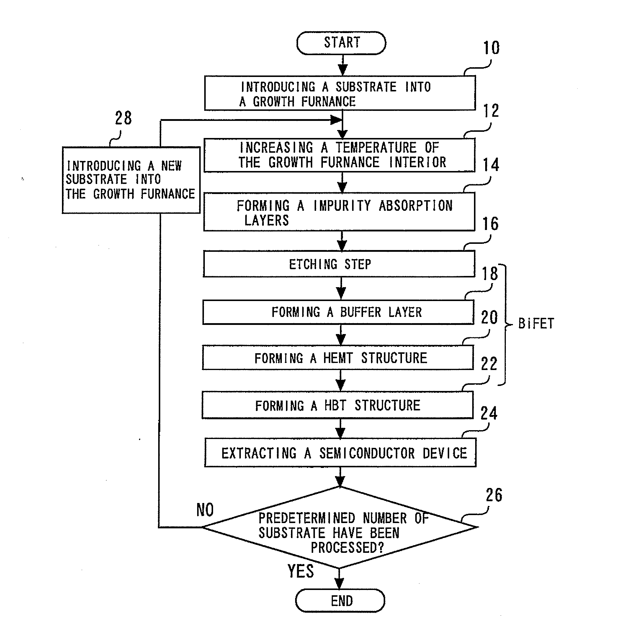
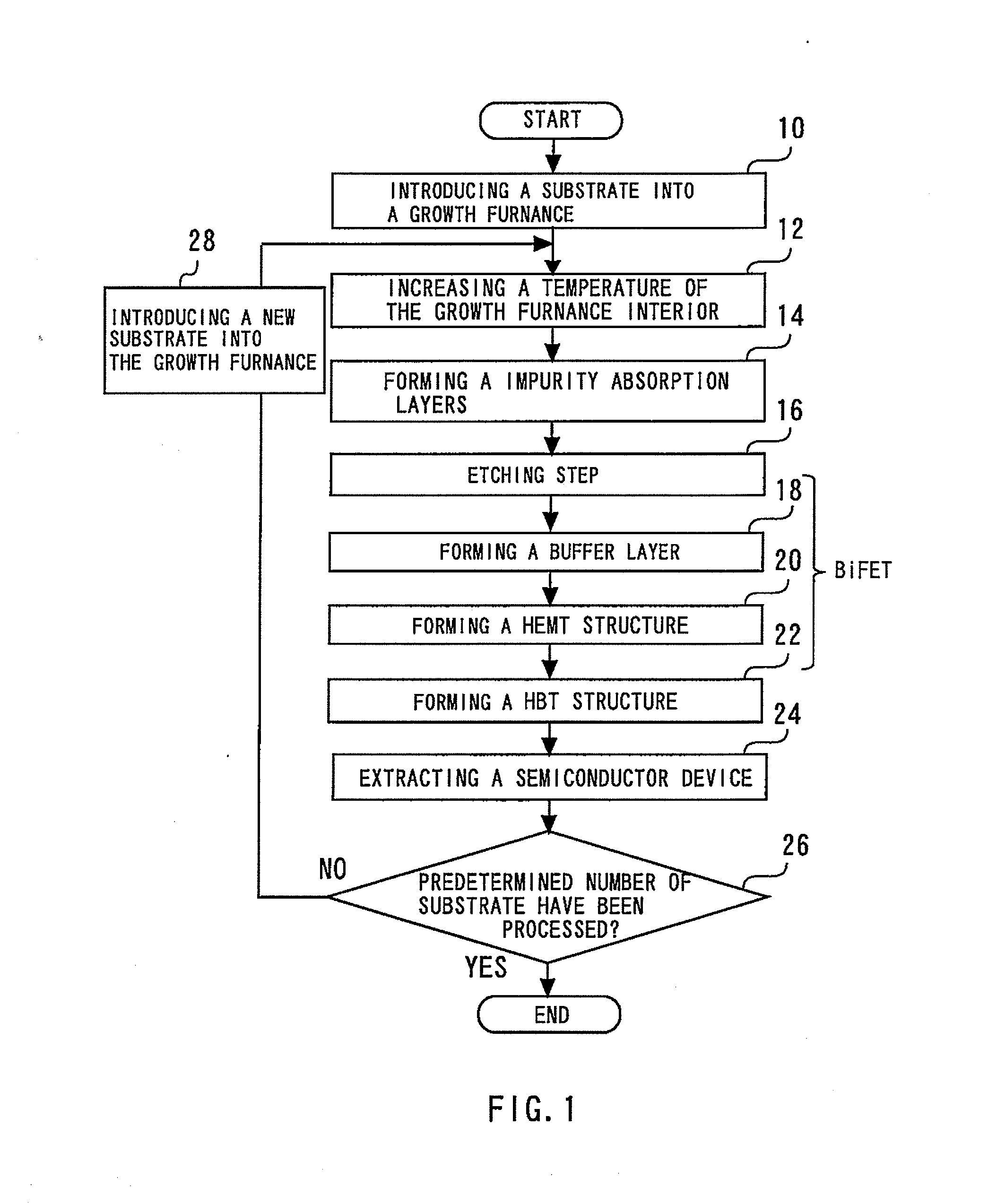
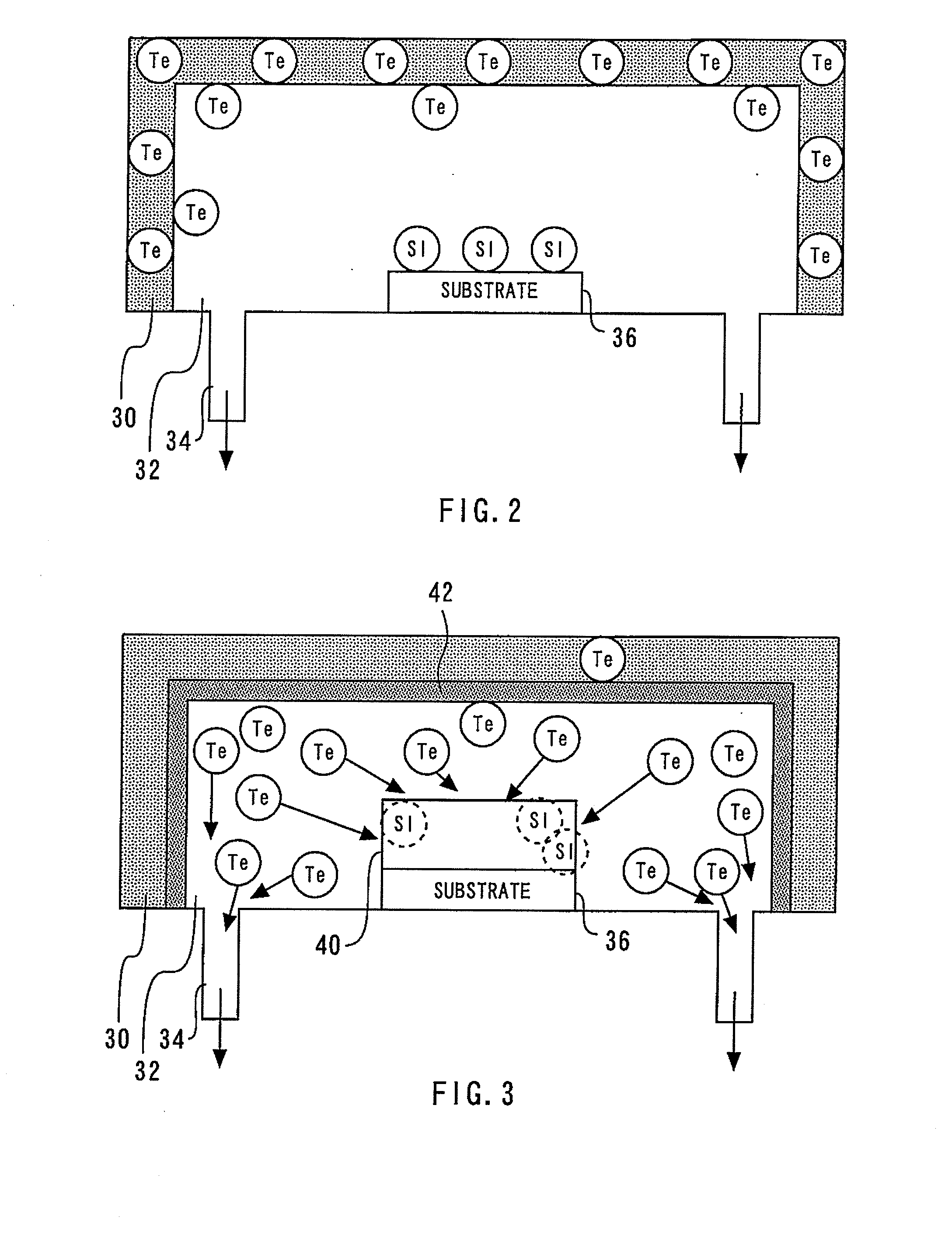
[0024]FIG. 1 is a flowchart showing a method of manufacturing a semiconductor device in accordance with a first embodiment of the present invention. The method of manufacturing a semiconductor device in accordance with the first embodiment will be described by following this flowchart and with reference at times to other drawings. First, a substrate is introduced into a growth furnace (step 10). This step is hereinafter referred to as the introduction step. FIG. 2 is a diagram showing the growth furnace and the substrate after the substrate has been introduced into the growth furnace. The growth furnace 30 is an MOCVD apparatus. Connection pipes 34 are coupled to the growth furnace 30 in order to evacuate the growth furnace interior space 32. The substrate 36 is formed of GaAs and is semi-insulating.

[0025]The growth furnace 30 has Te (tellurium) adhering thereto as a result of treatment performed in the growth furnace interior space 32 before the substrate 36 was introduced into the...

second embodiment

[0038]A method of manufacturing a semiconductor device in accordance with a second embodiment of the present invention can reduce the impurities present in the growth furnace by an amount greater than that achievable by the semiconductor device manufacturing method of the first embodiment described above, although these methods follow the same basic process steps. The following description is directed to the semiconductor device manufacturing method of the second embodiment, but does not include features common to the first embodiment.

[0039]FIG. 8 is a diagram showing getter members disposed around the substrate in accordance with the second embodiment. Specifically, the getter members 70 are disposed around the substrate 36. The getter members 70 serve to absorb impurities. FIG. 9 is a diagram showing the growth furnace and the substrate and the getter members disposed in the growth furnace. Each getter member 70 includes a dummy substrate 70a. The dummy substrate 70a is formed of ...


PUM

PropertyMeasurementUnit
temperatureaaaaaaaaaa
thicknessaaaaaaaaaa

Abstract

A method of manufacturing a semiconductor device, includes introducing a substrate into a growth furnace, forming impurity absorption layers on the substrate and on inner walls of the growth furnace, the impurity absorption layers absorbing impurities on a surface of the substrate and impurities in the growth furnace, etching and removing the impurity absorption layers and a portion of the substrate to produce a thinned substrate, forming a buffer layer on the thinned substrate, and forming semiconductor layers on the buffer layer.

Description

BACKGROUND OF THE INVENTION[0001]1. Field of the Invention[0002]The present invention relates to a method of manufacturing semiconductor devices such as field effect transistors (FETs) and high electron mobility transistors (HEMTs) formed, e.g., of Group III-V compound semiconductor.[0003]2. Background Art[0004]Japanese Laid-Open Patent Publication No. 2003-243308 discloses a technique for forming a dummy layer on a multilayer structure. The dummy layer serves to getter or absorbs unwanted elements remaining in the growth furnace. The dummy layer is etched away after it has gettered unwanted elements.[0005]The semiconductor device manufacturing method disclosed in the above publication is disadvantageous in that, since the dummy layer is formed on the multilayer structure after forming the structure on the substrate, the impurities which adhered to the substrate before the crystal growth cannot be removed.SUMMARY OF THE INVENTION[0006]The present invention has been made to solve the...

Claims


Application Information

Patent Timeline
Patent Type & Authority Applications(United States)
IPC IPC(8): H01L21/322
CPCH01L21/02463H01L21/02546H01L21/8252H01L21/02658H01L21/0262
Inventor HATAKENAKA, SUSUMUKAWAZU, ZEMPEIKAWAHARA, HIROYUKINAGIRA, TAKASHI
Owner MITSUBISHI ELECTRIC CORP
Why Eureka
Try Eureka