Method for implanting a piezoelectric material

a piezoelectric material and implanting technology, applied in the field of radiofrequency telecommunications, can solve the problems of difficult industrialisation of this technique, inability to transfer thin films (less than one micrometre) and congestion of authorised frequency bands

Active Publication Date: 2013-05-09
COMMISSARIAT A LENERGIE ATOMIQUE ET AUX ENERGIES ALTERNATIVES +1
View PDF2 Cites 11 Cited by
  • Summary
  • Abstract
  • Description
  • Claims
  • Application Information

AI Technical Summary

Problems solved by technology

The growth of radiofrequency telecommunications for some ten years has led to congestion of the authorised frequency bands.
However, due to the implantation energies used, which are of several MeV, it is difficult to industrialise

Method used


Image

  • Method for implanting a piezoelectric material
  • Method for implanting a piezoelectric material
  • Method for implanting a piezoelectric material

Examples


Embodiment Construction

[0011]The invention firstly proposes a method of producing a structure made of a piezoelectric material, including:

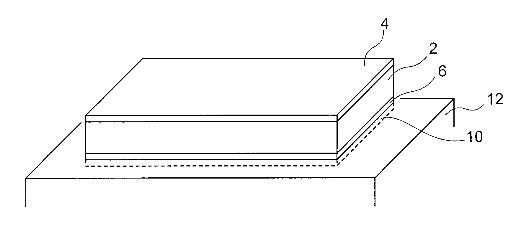
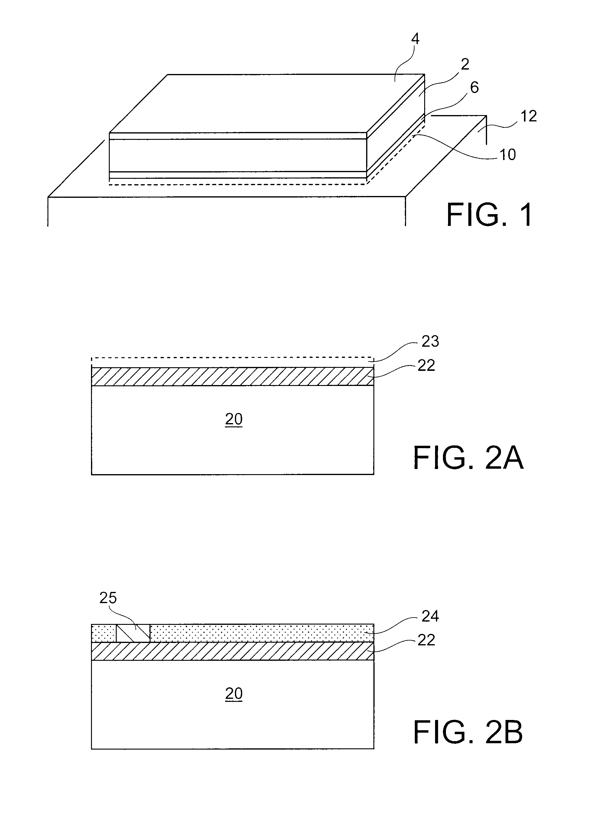
[0012]a) production of a stack including at least one metal layer and / or at least one surface layer which is conductive in electrical terms on a substrate made of piezoelectric material, for example LiNbO3 or LiTaO3, where at least one electrical contact is established between the conductive layer and a metal element outside the stack,

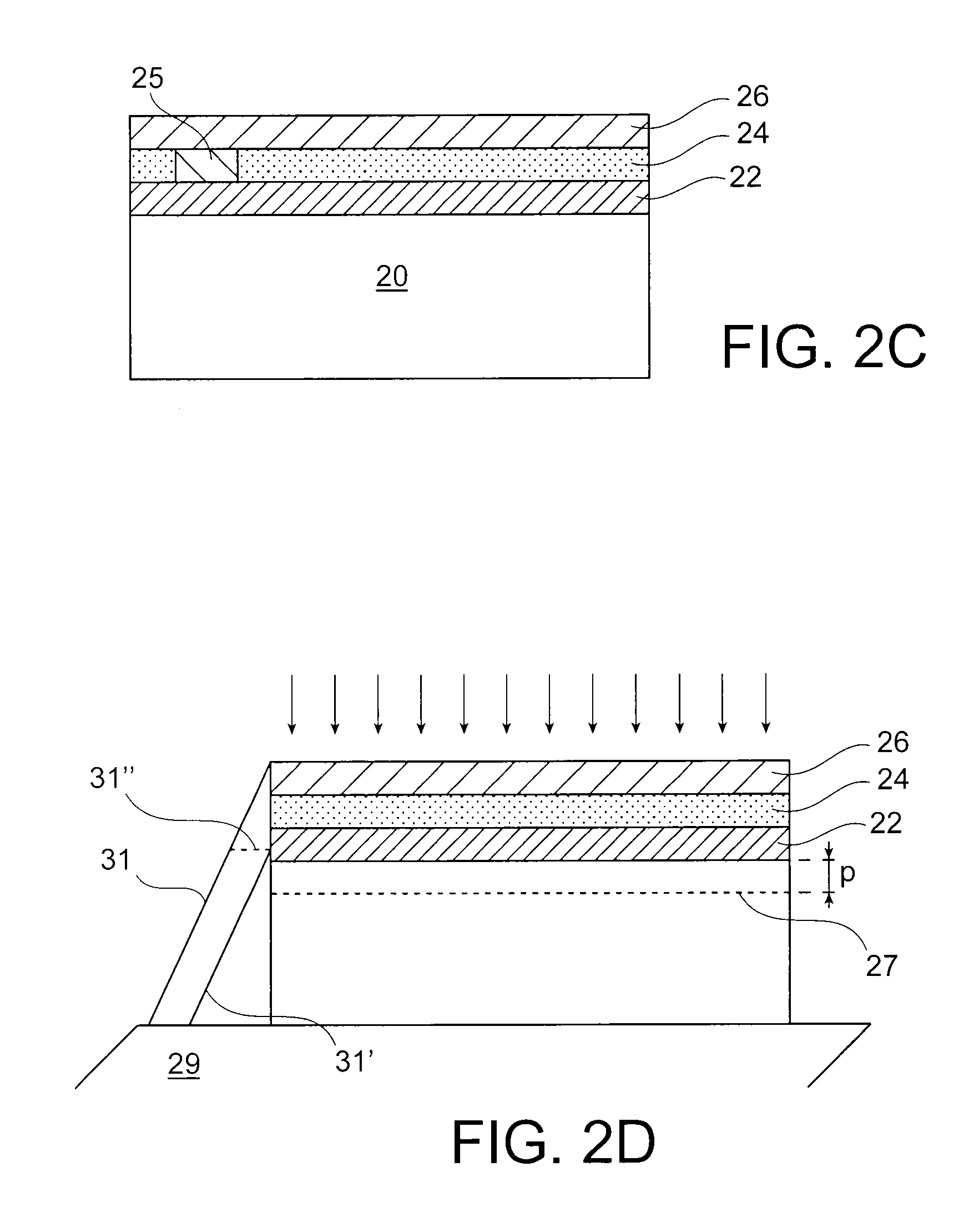
[0013]b) an implantation of one or more gaseous species, through at least the said conductive layer and the metal layer, to form an embrittlement area in the piezoelectric substrate,

[0014]c) an assembly of the stack obtained in this manner with a transfer substrate, followed by fracturing of the piezoelectric substrate, in the embrittlement area, to form an assembly including at least one layer made of piezoelectric material, a metal layer and the transfer substrate.

[0015]The invention thus proposes a method enabling a substrate to be prod...


PUM

PropertyMeasurementUnit
Thicknessaaaaaaaaaa
Thicknessaaaaaaaaaa
Electrical conductivityaaaaaaaaaa

Abstract

A method of producing a structure made of a piezoelectric material, including: a) production of a stack including at least one metal layer and at least one conductive layer on a substrate made of piezoelectric material, wherein at least one electrical contact is established between the conductive layer and a metal element outside the stack; b) an ionic and/or atomic implantation, through the conductive layer and the metal layer; c) transfer of the substrate onto a transfer substrate, followed by fracturing of the transferred piezoelectric substrate, in an embrittlement area.

Description

TECHNICAL FIELD AND PRIOR ART[0001]The growth of radiofrequency telecommunications for some ten years has led to congestion of the authorised frequency bands. To take advantage of the available frequency ranges systems must include band filtering, with a narrow transition band. Only SAW (surface acoustic wave) or BAW (bulk acoustic wave) technology resonators, using the piezoelectric properties of the materials, enable these specifications to be met with low losses and a compact configuration. Currently, piezoelectric layers used for these filters are made by deposition (BAW filters) or from bulk substrates (SAW filters).[0002]A BAW is represented schematically in FIG. 1: it includes a fine piezoelectric layer 2 of the order of 1 μm thick positioned between two electrodes 4, 6.[0003]The assembly rests on a substrate 12, but may be insulated acoustically by means 10. The acoustic insulation may be obtained either by suspending the piezoelectric film above a cavity (FBAR technology), ...

Claims


Application Information

Patent Timeline
IPC IPC(8): H01L41/22H01L41/312
CPCH03H3/02H03H9/131Y10T29/42H01L41/313H01L41/22H10N30/073H10N30/01
Inventor DEGUET, CHRYSTELBLANC, NICOLASIMBERT, BRUNOMOULET, JEAN-SEBASTIEN
Owner COMMISSARIAT A LENERGIE ATOMIQUE ET AUX ENERGIES ALTERNATIVES
Why Eureka
Try Eureka