
Magnetic tunnel junction devices having magnetic layers formed on composite, obliquely deposited seed layers

a tunnel junction and composite technology, applied in semiconductor devices, digital storage, instruments, etc., can solve the problems of inability to reduce values, inability to make tunnel barriers too thin, and inability to reduce write current, etc., to achieve the effect of increasing the in-plane magnetic anisotropy hk

Inactive Publication Date: 2013-05-16
IBM CORP
View PDF11 Cites 43 Cited by
  • Summary
  • Abstract
  • Description
  • Claims
  • Application Information

AI Technical Summary

Benefits of technology

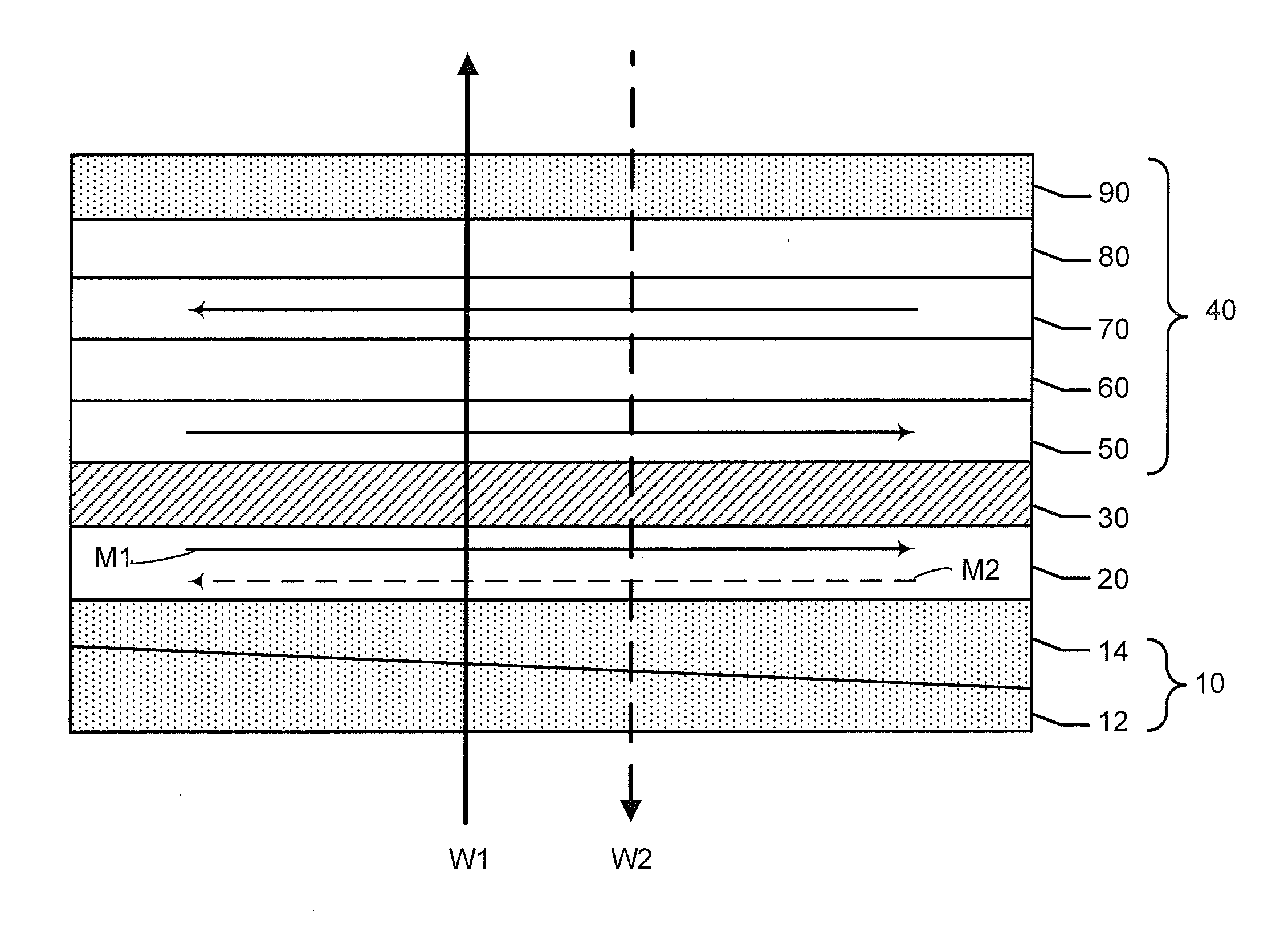
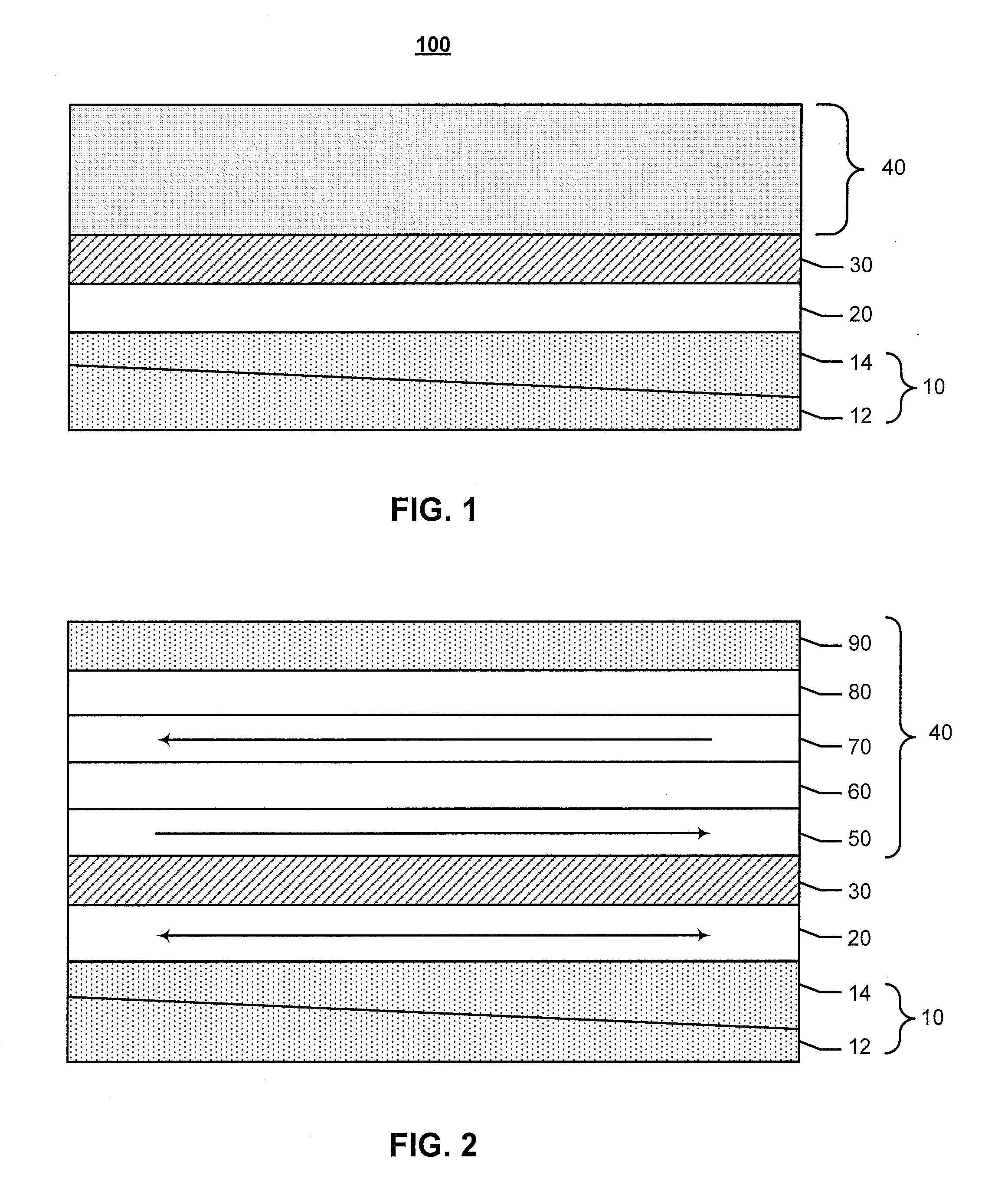
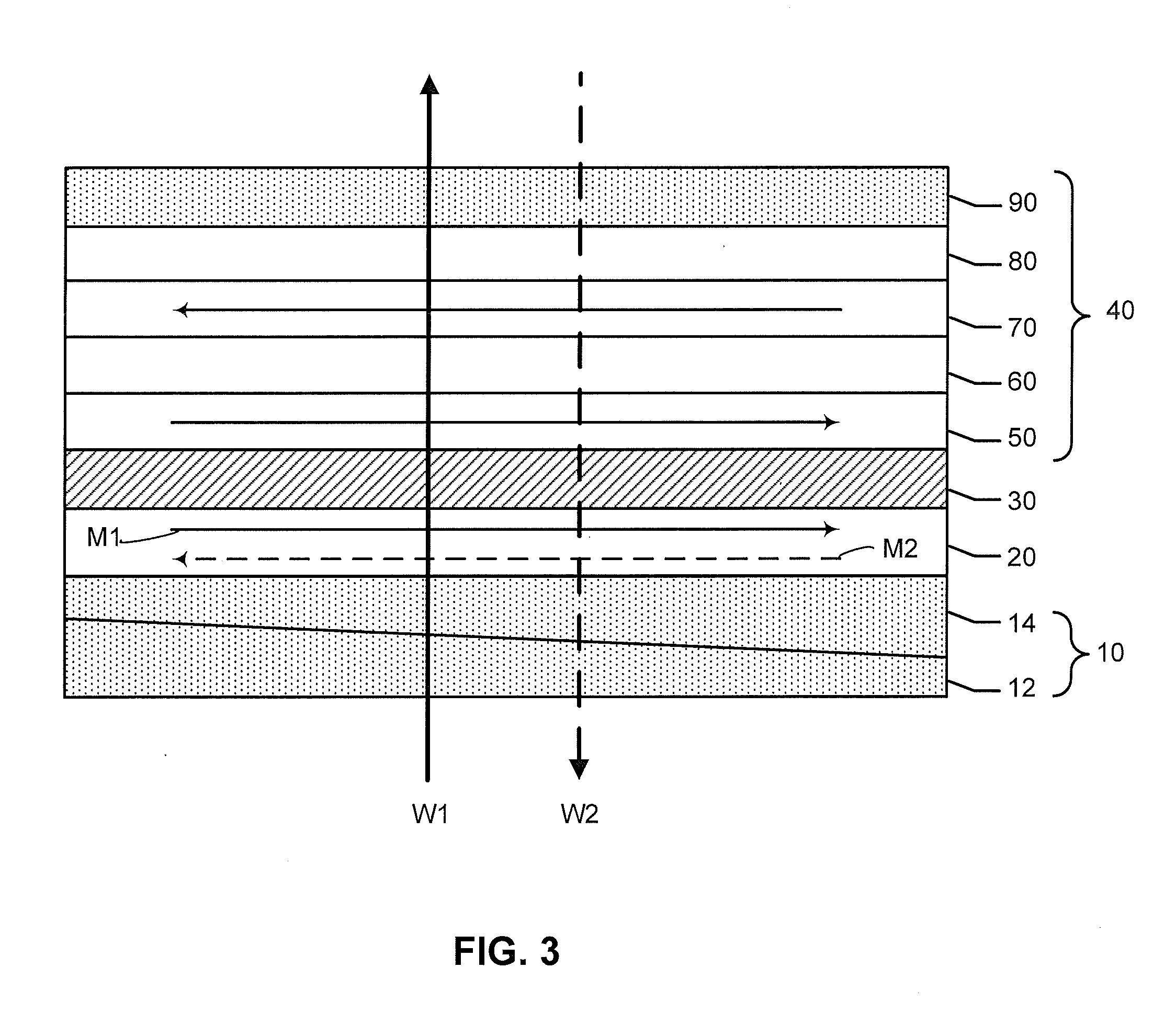
The invention relates to a method for improving the magnetic anisotropy of magnetic layers in semiconductor devices, such as magnetic tunnel junctions. This is achieved by depositing a composite seed layer with an incident angle between 15 degrees and 25 degrees on a substrate, followed by the growth of a magnetic layer on top of the composite seed layer. The composite seed layer consists of two layers, one layer deposited in a first direction and another layer deposited in a second direction opposite to the first direction. The magnetic layer is made of a composition of Co and Fe. The method results in a more stable magnetic anisotropy of the magnetic layer, which is important for the performance of magnetic tunnel junctions in semiconductor devices.

Problems solved by technology

Spin torque MRAM technology faces several challenges before it can become practical for manufacture and implementation of MRAM memory devices A key issue is the need to reduce the write current needed to switch the MTJ structure of the MRAM device between low and high resistive states (between logic low and high levels).
However, the tunnel barrier cannot be made too thin because of potential damage or breakdown (hole formation) of the material layer.
In this regard, it is not feasibly practical to reduce the values of
However, a reduction in the thickness, t, of the magnetic free layer, will result in a reduced activation energy Ea, which is undesirable.

Method used


Image

  • Magnetic tunnel junction devices having magnetic layers formed on composite, obliquely deposited seed layers
  • Magnetic tunnel junction devices having magnetic layers formed on composite, obliquely deposited seed layers
  • Magnetic tunnel junction devices having magnetic layers formed on composite, obliquely deposited seed layers

Examples


Embodiment Construction

[0021]Preferred embodiments of the invention will now be described in further detail with reference to semiconductor stack structures and magnetic tunnel junction (MTJ) structures that are constructed having a magnetic free layer formed on composite, obliquely deposited seed layers, which results in increased in-plane magnetic anisotropy of the magnetic free layer.

[0022]It has been previously reported that a large in-plane anisotropy can be induced in a magnetic free layer in a stack structure formed by obliquely depositing a seed layer of Ru (ruthenium) at a large incidence angle of 60 degrees (angle between the incident beam and the surface normal of the substrate), followed by depositing magnetic material consisting of Fe90Co10 or Fe10Co90, and followed by depositing a Ru cap layer. See Z. Lu, et al. “Magnetic Anisotropy of FeCo Films induced by Obliquely Sputtered Ru Underlayers,” IEEE Trans. Mag. 45, 4008 (2009). In practice, construction of this magnetic stack structure is not...


PUM


Abstract

Semiconductor stack structures such as magnetic tunnel junction structures having a magnetic free layer that is grown on composite, obliquely deposited seed layers to induce an increased in-plane magnetic anisotropy Hk of the magnetic free layer. In one aspect, a semiconductor device includes a composite seed layer formed on a substrate, and a magnetic layer formed on the composite seed layer. The composite seed layer includes a first seed layer obliquely formed with an incident angle from a surface normal of the substrate along a first direction of the substrate, and a second seed layer obliquely formed with the incident angle on the first seed layer along a second direction of the substrate, opposite the first direction.

Description

TECHNICAL FIELD[0001]This invention relates generally to magnetic tunnel junction (MTJ) structures for use with electronic components such as spin torque MRAM (magnetoresistive random access memory) and other magnetoresistive structures and more specifically, to magnetic tunnel junction structures having a magnetic free layer that is grown on composite, obliquely deposited seed layers to induce an increased in-plane magnetic anisotropy of the magnetic free layer for MTJ structures.BACKGROUND[0002]As is known in the art, a basic component of an MTJ device is a sandwich of two thin ferromagnetic (and / or ferrimagnetic) layers (magnetic free layer and a magnetic pinned layers) separated by a very thin insulating layer (tunnel barrier layer) through which electrons can tunnel. The tunneling current is typically higher when the magnetic moments of the magnetic free and pinned layers are parallel (oriented in same direction) and lower when the magnetic moments of the magnetic free and pinn...

Claims


Application Information

Patent Timeline
IPC IPC(8): H01L29/82H01L21/02
CPCH01L43/08H01L27/228H01L43/12G11C11/161H10B61/22H10N50/10H10N50/01
Inventor VETRFRANCESCO A.WORLEDGE, DANIEL C.
Owner IBM CORP
Learn More