Power Semiconductor Unit, Power Module, Power Semiconductor Unit Manufacturing Method, and Power Module Manufacturing Method
a technology of power semiconductor and manufacturing method, which is applied in the direction of battery/cell propulsion, electric devices, transportation and packaging, etc., can solve the problems of difficult control and drive of large-capacity motors mounted thereon, and achieve the effect of improving reliability and preventing void generation
- Summary
- Abstract
- Description
- Claims
- Application Information
AI Technical Summary
Benefits of technology
Problems solved by technology
Method used
Image
Examples
first embodiment
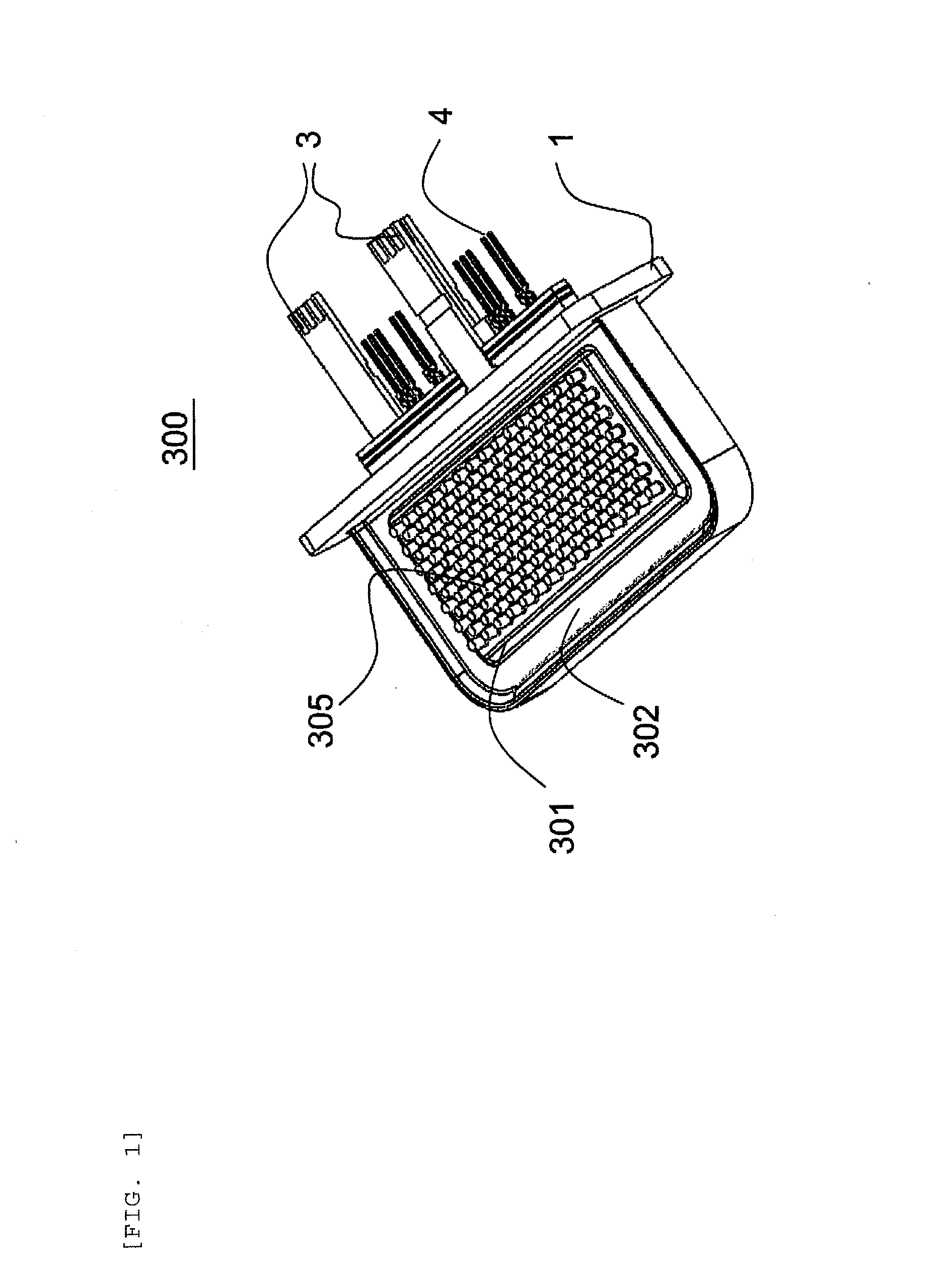
[0047]FIG. 1 illustrates the external appearance of a power module according to the invention. A power module 300 includes a power semiconductor unit formed by transfer molding in such a shape as to accommodate switching elements, and housed within a metal case 1. The power module 300 is incorporated in a power converter mounted on an electric vehicle such as an electric automobile and a hybrid automobile.
[0048]Each of the side surfaces of the metal case 1 has a thick portion 301 from which a plurality of heat radiation fins 305 project, and a thin portion 302 surrounding the thick portion 301. As will be explained below, the heat radiation surface of the power semiconductor unit housed inside and the inner circumferential surface of the thick portion 301 are brought into close contact with each other by plastic deformation of the thin portion 302. Major current terminals 3 and signal terminals 4 provided on the power semiconductor unit project from one surface of the metal case 1.
[...
second embodiment
[0135]A second embodiment according to the invention is hereinafter described with reference to FIGS. 22 through 25. FIG. 22 schematically illustrates a cross section of a power module 300B according to the second embodiment. The difference between the power module 300B and the power module 300 shown in FIG. 12 is the shape of the electrode lead frame 7. This different point is chiefly discussed in the following explanation.
[0136]Similarly to the first embodiment, the power semiconductor unit 6 is housed in the metal case 1, and the insulation sheets 10 are disposed between the power semiconductor unit 6 and the metal case 1. The electrode lead frame 7 has a solder injection hole 41 which penetrates the electrode lead frame 7. In the manufacture of the power semiconductor unit 6, the collector side electrode of the power semiconductor element 5 and the electrode lead frame 7 are joined by solder injected through the injection hole 41. A groove 44 is formed in the heat radiation surf...
PUM
 Abstract
Description
Claims
Application Information


