Electro-optical device and electronic apparatus

a technology of optical devices and electronic devices, applied in static indicating devices, instruments, optical elements, etc., can solve the problems of adversely affecting the uniformity of display screen, difficult to output data signals with extremely fine precision, and difficult to narrow the pitch of data lines. , to achieve the effect of narrowing the pitch of data lines

Active Publication Date: 2013-05-16
SEIKO EPSON CORP
View PDF4 Cites 43 Cited by
  • Summary
  • Abstract
  • Description
  • Claims
  • Application Information

AI Technical Summary

Benefits of technology

[0009]An advantage of some aspects of the invention is that it provides an electro-optical device and an electronic

Problems solved by technology

At this time, if the characteristics of the threshold voltages or the like of the transistors are varied for each pixel circuit, display unevenness adversely affecting the uniformity of the display screen is generated.
In a circuit having a high driving capability in this manner, it is difficult to output the data signal with

Method used


Image

  • Electro-optical device and electronic apparatus
  • Electro-optical device and electronic apparatus
  • Electro-optical device and electronic apparatus

Examples


application and modification examples

[0164]The invention is not limited to embodiments such as the above-described embodiments and application examples, and, for example, various modifications are possible as described in the following. Further, one or a plurality of arbitrarily selected forms of the modifications described below can also be combined as appropriate.

Structure of Electro-Optical Device

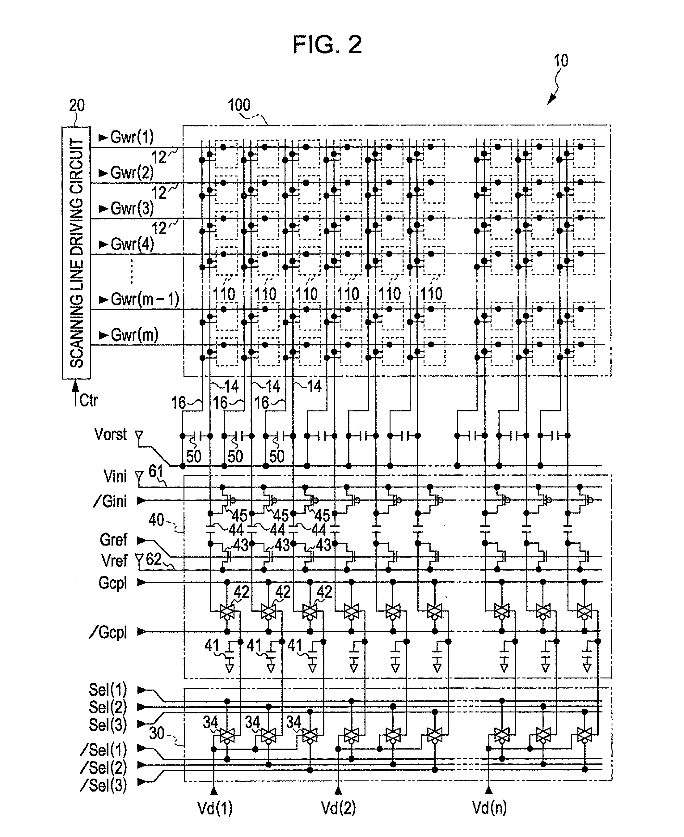
[0165]In the above-described first to fourth aspects, the connection wirings 189, 191, 196, and 201 were used; however, a part or all of these may be omitted and direct connection may be made to the member which is the target of the connection. In such a case, the common electrode 118 or the wiring 250 and the electrode 412b are set in common and the electrode 412b may be omitted. Further, the electrode 412b and the electrode 411b are set in common and the electrode 411b may be omitted. Further, the wiring 211 and the wiring 195 are made to be in common and the wiring 195 may be omitted. Furthermore, the wiring 194 and the ...


PUM


Abstract

An electro-optical device comprises a substrate, a scanning line, a data line, a pixel circuit, and a first storage capacitor holding a first voltage corresponding to a data signal. The first storage capacitor includes a first portion and a second portion connected in parallel. The first portion and the second portion overlap when viewed from a direction orthogonal with respect to the first main surface.

Description

BACKGROUND[0001]1. Technical Field[0002]The present invention relates to an electro-optical device and an electronic apparatus useful when miniaturizing a pixel circuit, for example.[0003]2. Related Art[0004]In recent years, various types of electro-optical devices using light-emitting elements such as organic light-emitting diodes (below, “OLED”) have been proposed. In such electro-optical devices, pixel circuits including the above-described light-emitting elements, transistors, and the like corresponding to intersections of scanning lines and data lines are generally configured to be provided corresponding to the pixels of the image to be displayed. In such a configuration, when a data signal of a potential according to the gradation level of the pixels is applied to the gate of the transistor, the transistor supplies current according to the voltage between the gate and the source to the light-emitting element. In this manner, the light-emitting element emits light with a lumina...

Claims


Application Information

Patent Timeline
IPC IPC(8): H01L33/08G09G3/30G06F3/038
CPCG09G3/3233G06F3/038G09G2300/0861H10K59/123H10K59/131H10K59/1216G02B27/017G02B2027/0178G09G3/3208G09G3/3258G09G3/3266G09G3/3291
Inventor KUBOTA, TAKEHIKONOMURA, TAKESHIOTA, HITOSHI
Owner SEIKO EPSON CORP
Why Eureka
Try Eureka