IC embedded substrate and method of manufacturing the same

a technology of embedded substrates and substrates, which is applied in the direction of printed circuits, semiconductor devices, semiconductor/solid-state device details, etc., can solve the problems of reducing the length of the via-hole conductor that is connected to the pad electrode, the adhesive strength the flatness of the upper surface of the insulating layer could be worsened, and the reliability of the wiring layer formed on the upper surface of the insulating layer could be reduced,

Active Publication Date: 2015-05-28
TDK CORPARATION
View PDF1 Cites 21 Cited by
  • Summary
  • Abstract
  • Description
  • Claims
  • Application Information

AI Technical Summary

Benefits of technology

[0012]According to the present invention, it is preferred that the core substrate be a resin substrate containing a fibrous reinforcing material, and the lower insulating layer and the upper insulating layer be a resin layer not containing a fibrous reinforcing material. According to this configuration, the IC embedded substrate that combines high substrate strength and thinness can be realized.
[0013]According to the present invention, it is preferred that an entirety of the upper surface of the core substrate be in contact with the upper insulating layer, and an entirety of a lower surface of the core substrate be in contact with the lower insulating layer. According to this configuration, it is possible to realize what is known as a two-layer IC embedded substrate, which combines high substrate strength and thinness.
[0014]According to the present invention, it is preferred that the lower insulating layer be substantially uniform in thickness, and the core substrate be thinner than the IC chip. According to this configuration, the upper insulating layer located above the IC chip can be made thinner. Therefore, the length of a via-hole conductor that is connected to a pad electrode of the IC chip by passing through the upper insulating layer can be reliably shortened.
[0015]According to the present invention, it is preferred that, at least at one of four corners of the IC chip, the gap between the side surface of the IC chip and the inner peripheral surface of the opening of the core substrate be partially widened in width. This configuration makes it easier for resin to flow into the gap, improving the filling performance of the resin. As a result, the positional deviation of the IC chip is reduced, and the bonding strength of the IC chip against the lower insulating layer is increased.
[0016]A method of manufacturing an IC embedded substrate of the present invention includes: a step of forming a lower insulating layer on an upper surface of a lower conductor layer formed on an upper surface of a carrier; a step of mounting a core substrate and an IC chip, which is thicker than the core substrate, on the upper surface of the lower insulating layer in such a way that the IC chip is housed in an opening of the core substrate that includes the opening; a step of forming an upper insulating layer that covers an upper surface of the IC chip and an upper surface of the core substrate; a step of forming an upper conductor layer on an upper surface of the upper insulating layer; and a step of forming a via-hole conductor that passes through the upper insulating layer to connect the IC chip and the upper conductor layer, wherein the step of forming the upper insulating layer includes a step of filling a gap between a side surface of the IC chip and an inner peripheral surface of the opening of the core substrate.
[0017]According to the present invention, it is possible to produce an IC embedded substrate that includes a high-rigidity core substrate, is high in handling ability, and combines high substrate strength and thinness. Moreover, since the length of a via-hole conductor that is connected to a pad electrode of the IC chip by passing through the upper insulating layer is short, it is possible to produce an IC embedded substrate that has via-hole conductors of small-diameter and narrow pitch. Moreover, the upper surface of the core substrate is lower than the upper surface of the IC chip. Therefore, even if dust is adhering to the upper surface of the IC chip, the dust will flow and move toward the core substrate (downward) together with the resin at a time when the IC chip is embedded in the upper insulating layer. Therefore, it is possible to prevent a connection or insulation failure of the IC chip. Shards of glass cloth or the like held by the core substrate are unlikely to stay on the IC chip, and similar advantageous effects can be expected. This action is also effective for a filler contained in the resin. By performing hot pressing in such a way as to prevent a relatively large filler from remaining on the top of the IC chip, it is also expected to prevent quality abnormality associated with the resin that has been made thinner.

Problems solved by technology

However, in the case of the above conventional embedded substrate, the following problems arise, as the core substrate is almost equal in thickness to the IC chip.
Therefore, the problem is that it is difficult to reduce the size of via-hole conductors and narrow their pitch.
However, in this case, the problem is that the adhesive strength of the insulating layer and the flatness of the upper surface of the insulating layer could be worsened, and the reliability of a wiring layer formed on the upper surface of the insulating layer would decrease.
The problem will become more obvious especially when the size of a filler contained in the insulating layer is larger than the thickness of the cured resin.
However, in such a case, the gap between a side surface of the IC chip and the inner peripheral surface of the cavity is very narrow, making it difficult to fill the gap with resin.
If the gap is not sufficiently filled with resin, the fixed IC chip could become unstable, possibly leading to positional deviation of the IC chip and a connection failure.

Method used


Image

  • IC embedded substrate and method of manufacturing the same
  • IC embedded substrate and method of manufacturing the same
  • IC embedded substrate and method of manufacturing the same

Examples


first embodiment

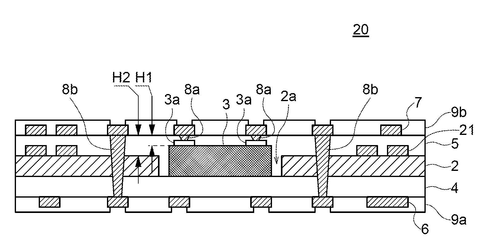
[0029]FIG. 1 is a schematic cross-sectional view showing the configuration of an IC embedded substrate according to the present invention.

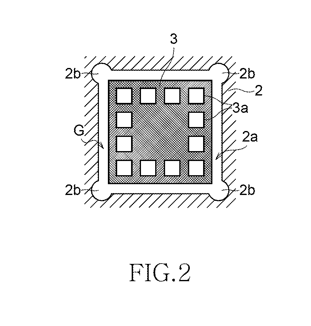
[0030]As shown in FIG. 1, an IC embedded substrate 1 of the present embodiment includes a core substrate 2, which has an opening 2a; an IC chip 3, which is provided within the opening 2a; a lower insulating layer 4, which covers the lower surfaces of the core substrate 2 and IC chip 3; an upper insulating layer 5, which covers the upper surfaces of the core substrate 2 and IC chip 3; a lower wiring layer 6, which is formed on the lower surface of the lower insulating layer 4; and an upper wiring layer 7, which is formed on the upper surface of the upper insulating layer 5. Throughout this specification, the “IC embedded substrate” includes not only an individual substrate (individual piece, individual product) that is a unit substrate in which IC chips are embedded, but also a collective substrate (work board, work sheet) that includes a plurality...

second embodiment

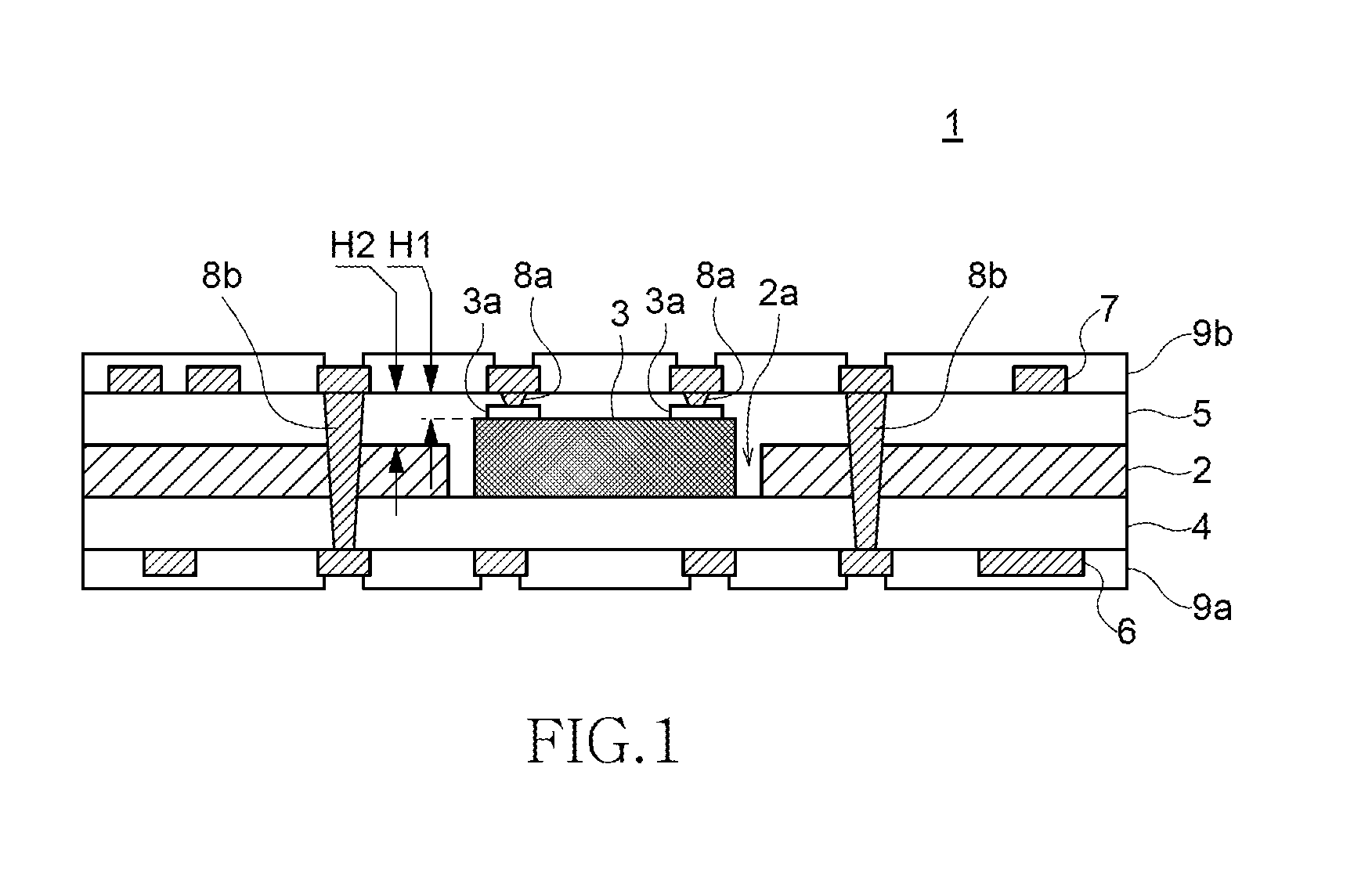
[0063]FIG. 7 is a schematic cross-sectional view showing the configuration of an IC embedded substrate according to the present invention.

[0064]As shown in FIG. 7, an IC embedded substrate 20 of the present embodiment is characterized by a conductor pattern of an internal wiring layer 21 that is provided on the upper surface of the core substrate 2. The above-described IC embedded substrate 1 of the first embodiment is a so-called two-layer substrate with no internal wiring layer. The IC embedded substrate 20 of the present embodiment is a multilayer substrate (three-layer substrate) with an internal wiring layer. In this manner, the IC embedded substrate of the present invention can be formed as a multilayer substrate.

[0065]It is apparent that the present invention is not limited to the above embodiments, but may be modified and changed without departing from the scope and spirit of the invention.

[0066]For example, in the case of the above embodiments, after the IC chip 3 is mounte...


PUM


Abstract

Disclosed herein is an IC embedded substrate that includes a core substrate having an opening, an IC chip provided in the opening, a lower insulating layer, and upper insulating layer. The IC chip and the core substrate is sandwiched between the lower insulating layer and the upper insulating layer. The upper insulating layer is formed in such a way as to fill a gap between a side surface of the IC chip and an inner peripheral surface of the opening of the core substrate. A first distance from the upper surface of the IC chip to an upper surface of the upper insulating layer is shorter than a second distance from the upper surface of the core substrate to the upper surface of the upper insulating layer.

Description

BACKGROUND OF THE INVENTION[0001]1. Field of the Invention[0002]The present invention relates to an IC embedded substrate in which an IC chip is incorporated therein, and a method of manufacturing the IC embedded substrate.[0003]2. Description of Related Art[0004]In recent years, portable electronic devices, such as smartphones and tablet PCs, have become increasingly popular. In each of portable electronic devices, in order to reduce the size of the device and improve the functionality, an IC embedded substrate in which many functions are put together are mounted. The IC embedded substrate is a module component in which a semiconductor IC of a bare chip state that has been ground so as to be very thin is embedded in the substrate, and passive components, such as capacitors, inductors, thermistors, and resistors, are surface-mounted on the surface of the substrate. This IC embedded substrate allows various power supply circuits and a plurality of wireless communication functions to ...

Claims


Application Information

Patent Timeline
Patent Type & Authority Applications(United States)
IPC IPC(8): H01L23/00H01L21/56
CPCH01L24/20H01L2224/4918H01L21/561H01L23/3121H01L2924/12042H01L2224/83132H01L23/544H01L24/03H01L24/05H01L24/83H05K1/185H01L2224/04105H01L2224/05647H01L2224/2919H01L2224/32225H01L2223/54426H01L2223/54486H01L2224/18H01L2924/00H01L2924/00014H01L23/5226H01L2924/01079
Inventor TSUYUTANI, KAZUTOSHIKATSUMATA, MASASHI
Owner TDK CORPARATION
Why Eureka
Try Eureka