Multilayered structure, multilayered structure array and method of manufacturing the same

a technology of multi-layered structures and arrays, applied in the direction of fixed capacitor details, device material selection, feed-through capacitors, etc., can solve the problems of degrading piezoelectric actuator performance, power becomes difficult to supply, and the electric impedance of the element rises, so as to achieve easy formation, improve productivity, and facilitate arranging

Inactive Publication Date: 2006-03-30
FUJIFILM HLDG CORP +1
View PDF5 Cites 22 Cited by
  • Summary
  • Abstract
  • Description
  • Claims
  • Application Information

AI Technical Summary

Benefits of technology

[0015] According to the present invention, coatings containing a metal material are formed on the end surfaces of internal electrodes to be insulated from side electrodes and the coatings are caused to have insulation. Therefore, insulating films can be made further thinner while maintaining the withstand voltage thereof. Further, coatings can be easily formed on the end surfaces of internal electrodes even in a region where the dist...

Problems solved by technology

In microfabrication of an element having opposed electrodes, since the smaller the area of the element is made, the smaller the capacity between the electrodes becomes, a problem that the electrical impedance of the element rises occurs.
For example, when the electrical impedance rises in a piezoelectric actuator, the impedance matching cannot be taken with a signal circuit for driving the piezoelectric actuator and power becomes difficult to be supplied, and thereby, the performance as the piezoelectric actuator is degraded.
On this account, there is a problem that stress is concentrated on the part and the part becomes easy to break.
Currently, the insulat...

Method used


Image

  • Multilayered structure, multilayered structure array and method of manufacturing the same
  • Multilayered structure, multilayered structure array and method of manufacturing the same
  • Multilayered structure, multilayered structure array and method of manufacturing the same

Examples


first embodiment

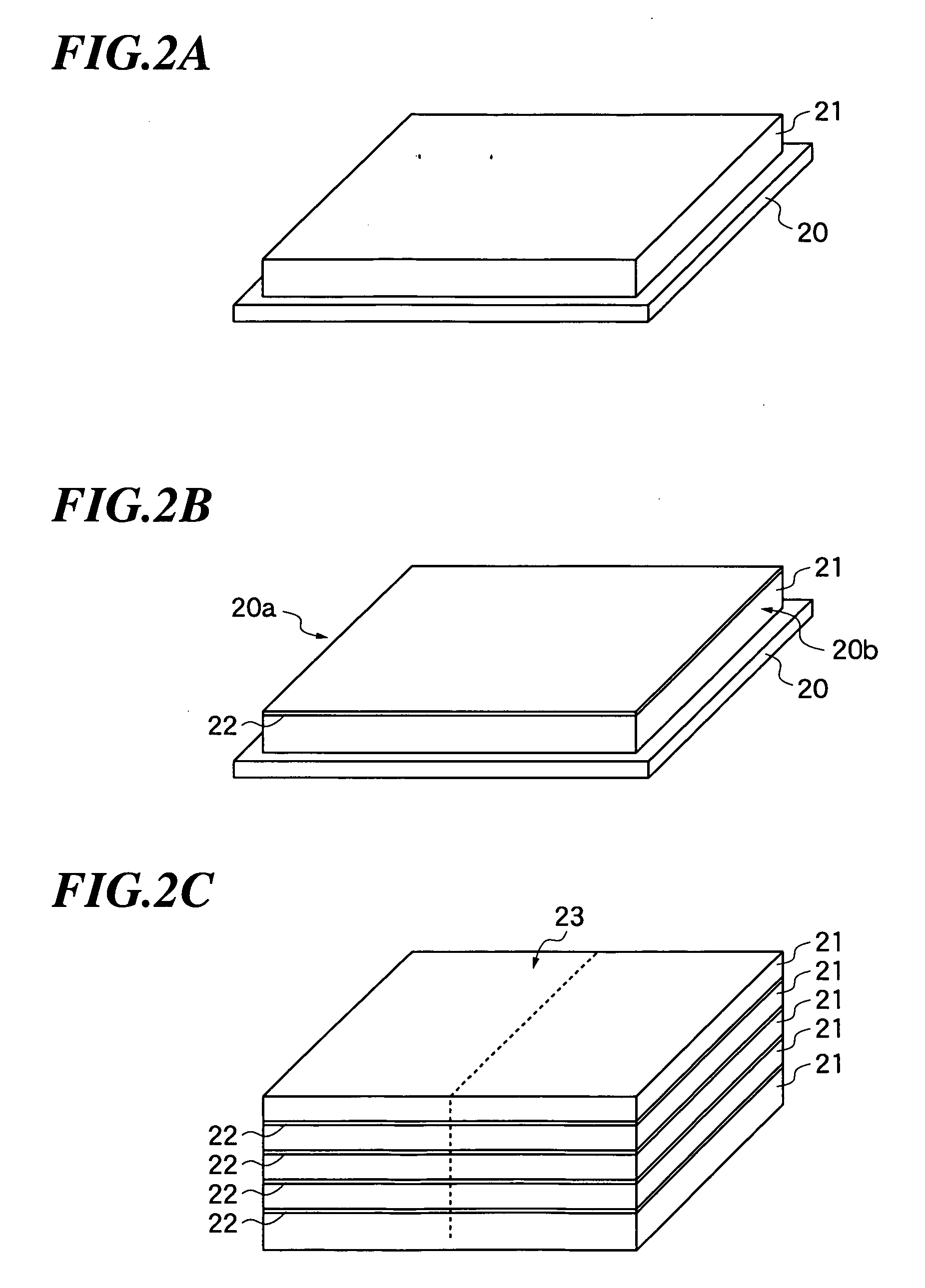
[0039] Next, a method of manufacturing a multilayered structure and a multilayered structure array according to the present invention will be described by referring to FIGS. 2A to 6C. FIGS. 2A to 6C are diagrams for explanation of the method of manufacturing a multilayered structure and a multilayered structure array according to the embodiment.

[0040] First, a workpiece in which plural piezoelectric material layers and plural electrode layers are stacked is fabricated. For the purpose, as shown in FIG. 2A, a piezoelectric material layer 21 is formed on a substrate 20. In this regard, in the embodiment, the aerosol deposition (AD) method is used. The AD method is a deposition method of spraying a raw material powder on a foundation layer at a high speed and depositing the raw material powder thereon, and also referred to as a gas deposition method, jet printing system, or injection deposition method.

[0041]FIG. 7 is a schematic diagram showing a film forming device by using the AD me...

second embodiment

[0068] Next, a multilayered structure according to the present invention will be described.

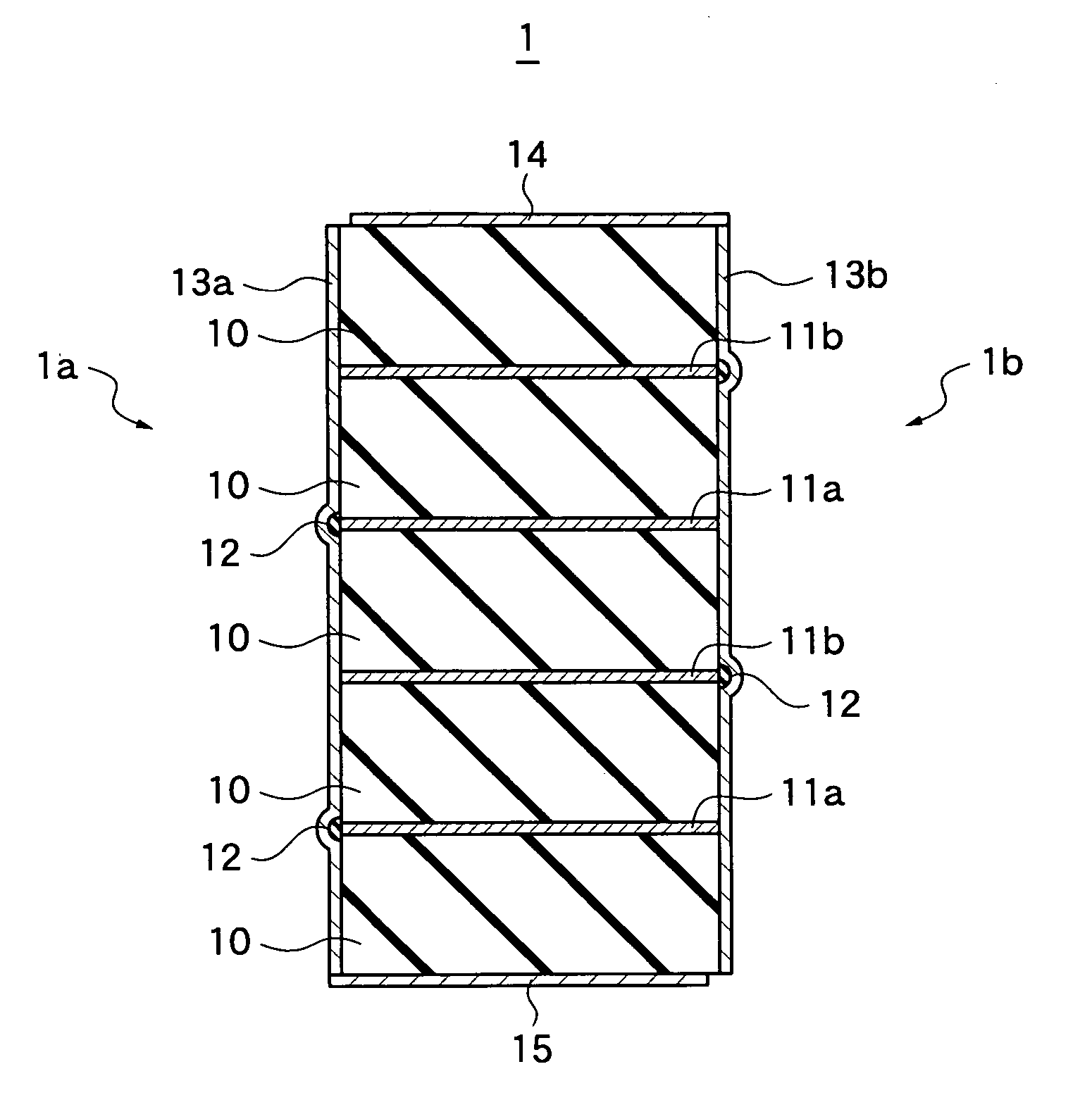
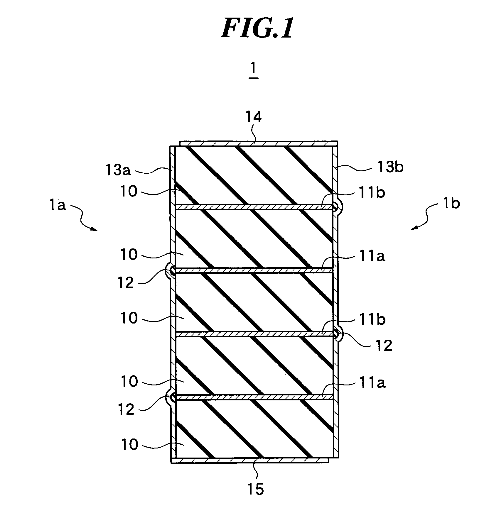
[0069]FIG. 9 is a sectional view showing a structure of the multilayered structure according to the second embodiment. This multilayered structure 3 has internal electrodes 11a and 11b in the multilayered structure 1 shown in FIG. 1 and, in place of the coatings 12, internal electrodes 61a and 61b and coatings 62. Other constitution is the same as that of the multilayered structure 1 shown in FIG. 1.

[0070] In the embodiment, the coatings 62 are formed by forming films of a conducting material on predetermined end surfaces of the internal electrode layers 61a and 61b, and then, making the films to have insulation by oxidizing them. However, the method of forming coatings differs from the method in the first embodiment. That is, in the embodiment, films are formed on the end surfaces of the internal electrode layers using magnetophoresis power in place of electrophoresis power. For this purpose...


PUM

PropertyMeasurementUnit
Fractionaaaaaaaaaa
Temperatureaaaaaaaaaa
Dielectric polarization enthalpyaaaaaaaaaa

Abstract

A multilayered structure array has narrow pitches by making thinner coatings for insulating internal electrode layers from side electrodes and the productivity of the multilayered structure array is improved. The multilayered structure includes: a first internal electrode layer; a piezoelectric layer formed on the first internal electrode layer; a second internal electrode layer formed on the piezoelectric layer; a first coating formed on an end surface of the first internal electrode layer in a first side surface region of the multilayered structure and containing one of metal oxide, metal nitride, metal fluoride and metal sulfide in at least one part thereof; and a second coating formed on an end surface of the second internal electrode layer in a second side surface region of the multilayered structure and containing one of metal oxide, metal nitride, metal fluoride and metal sulfide in at least one part thereof.

Description

BACKGROUND OF THE INVENTION [0001] 1. Field of the Invention [0002] The present invention relates to a multilayered structure in which insulating layers and electrode layers are alternately stacked, a multilayered structure array in which plural multilayered structures are arranged, and a method of manufacturing the multilayered structure or the multilayered structure array. [0003] 2. Description of a Related Art [0004] Multilayered structures, in each of which insulating (dielectric) layers and electrode layers are alternately formed, are utilized not only for multilayered capacitors but also for various uses such as piezoelectric pumps, piezoelectric actuators, and ultrasonic transducers. In recent years, with the developments of MEMS (micro electro mechanical systems) related devices, elements each having such a multilayered structure have been microfabricated still further and packaged more densely. [0005] In microfabrication of an element having opposed electrodes, since the sm...

Claims


Application Information

Patent Timeline
IPC IPC(8): H01G4/35H01L41/083H01L41/18H01L41/187H01L41/22H01L41/293H01L41/297H01L41/314H01L41/338H04R17/00H04R31/00
CPCH01G4/232H01L41/083H01L41/293Y10T29/435H01L27/20H01L41/0475H01L41/338H10N39/00H10N30/875H10N30/50H10N30/063H10N30/088
Inventor KUNIYASU, TOSHIAKI
Owner FUJIFILM HLDG CORP
Why Eureka
Try Eureka